3.1. Characterization of the As-Prepared Perovskite Films
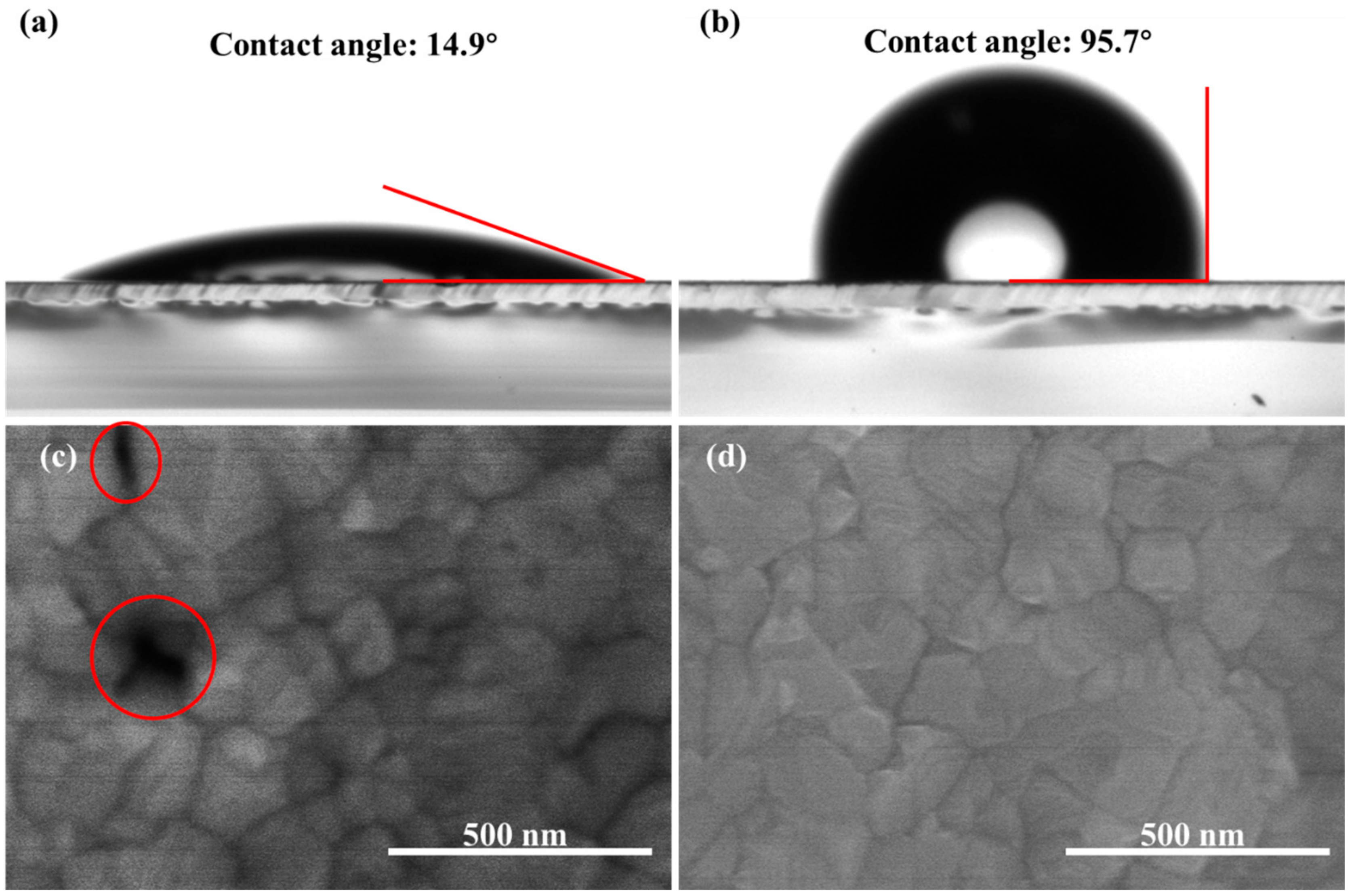
The hydrophobic property of the substrates is crucial for the nucleation of the perovskite [
8,
20]. Hence, the water contact angle images on the ITO and TPASBP surfaces were characterized, as shown in
Figure 1a,b. The contact angles of water on the two different surfaces were 14.9° and 95.7° for the ITO and TPASBP, respectively. The larger contact angle means that the TPASBP is much more hydrophobic than a bare ITO surface. Because of the hydrophobic property of TPASBP, it hardly dissolves in many polar solvents like GBL, DMSO,
N,
N-dimethylformamide (DMF), etc. (as shown in
Figure S1c). Hence, the hole-transporting layer and the CH
3NH
3PbI
3 layer can be fabricated consecutively on ITO by a solution process. Moreover, the top-view SEM images of the CH
3NH
3PbI
3 films on bare ITO and TPASBP (shown in
Figure 1c,d) revealed a clear correlation between the hydrophobic property of the substrate surface and the CH
3NH
3PbI
3 film morphology. It is obvious that there are clearly discerned pinholes in the perovskite film on bare ITO, whereas dense perovskite film without pinholes was obtained on TPASBP. Meanwhile, the average size of the CH
3NH
3PbI
3 grains on TPASBP was ∼203 nm, which was larger than that on ITO (average grain size ∼160 nm).
Figure S2 shows the corresponding grain size distribution of
Figure 1c,b. The morphologies of CH
3NH
3PbI
3 films on different substrates were further investigated by using AFM (as shown in
Figure S3), where the CH
3NH
3PbI
3 film based on hydrophobic TPASBP showed a smoother surface (root mean square (RMS) = 11.02 nm) relative to that on ITO (RMS = 14.69 nm). As shown in
Figure S4, compared to hydrophilic ITO, the hydrophobic surface of TPASBP induced a lower density of perovskite nuclei after spin-coating the perovskite precursor, thus promoting the perovskite to grow into compact films with large grains after thermal annealing. Meanwhile, due to the reduction of perovskite nuclei on the substrate, the heterogeneous nucleation of perovskite was suppressed, and a much smoother perovskite film was realized.
To gain further insight into the effect of hydrophobic TPASBP surfaces on CH
3NH
3PbI
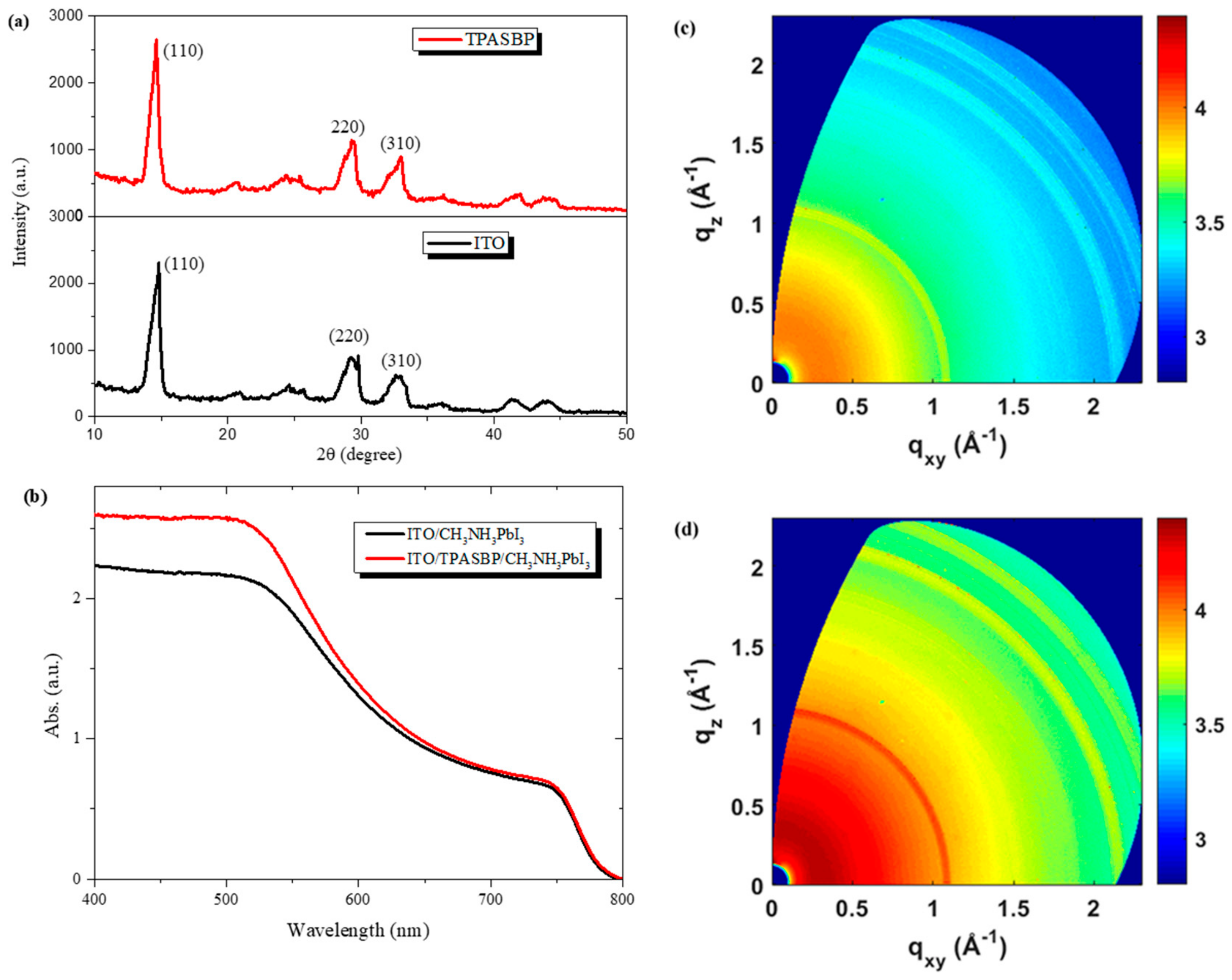
3 crystallization, the XRD patterns of CH
3NH
3PbI
3 films on ITO and TPASBP are shown in
Figure 2a. No significant change in the diffraction peak ratio was observed, indicating the same crystal orientation of CH
3NH
3PbI
3 film on both ITO and TPASBP. However, the X-ray diffraction peaks of CH
3NH
3PbI
3 (110), (220), and (310), were more intense and sharper for perovskite film on hydrophobic TPASBP. In addition, two-dimensional GIWAXS patterns of perovskite films on ITO and TPASBP were measured and are shown in
Figure 2c,d respectively. For the perovskite film deposited on TPASBP, the feature of CH
3NH
3PbI
3 crystalline domains was clearer and the two-dimensional GIWAXS pattern exhibited stronger intensity at the diffraction peaks, indicating that the perovskite film on TPASBP showed finer ordering structures and better crystallization than that on ITO. The results from XRD and GIWAXS imply that the crystallization of CH
3NH
3PbI
3 grown on the hydrophobic TPASBP was greatly improved in comparison with that on bare ITO. Hence, on the basis of improved CH
3NH
3PbI
3 morphology and crystallization, the light absorption of perovskite film on TPASBP is enhanced in the whole wavelength range from 400 to 800 nm, especially from 400 to 550 nm, as presented by the UV–vis absorption spectra of perovskite films on ITO and TPASBP in
Figure 2b.
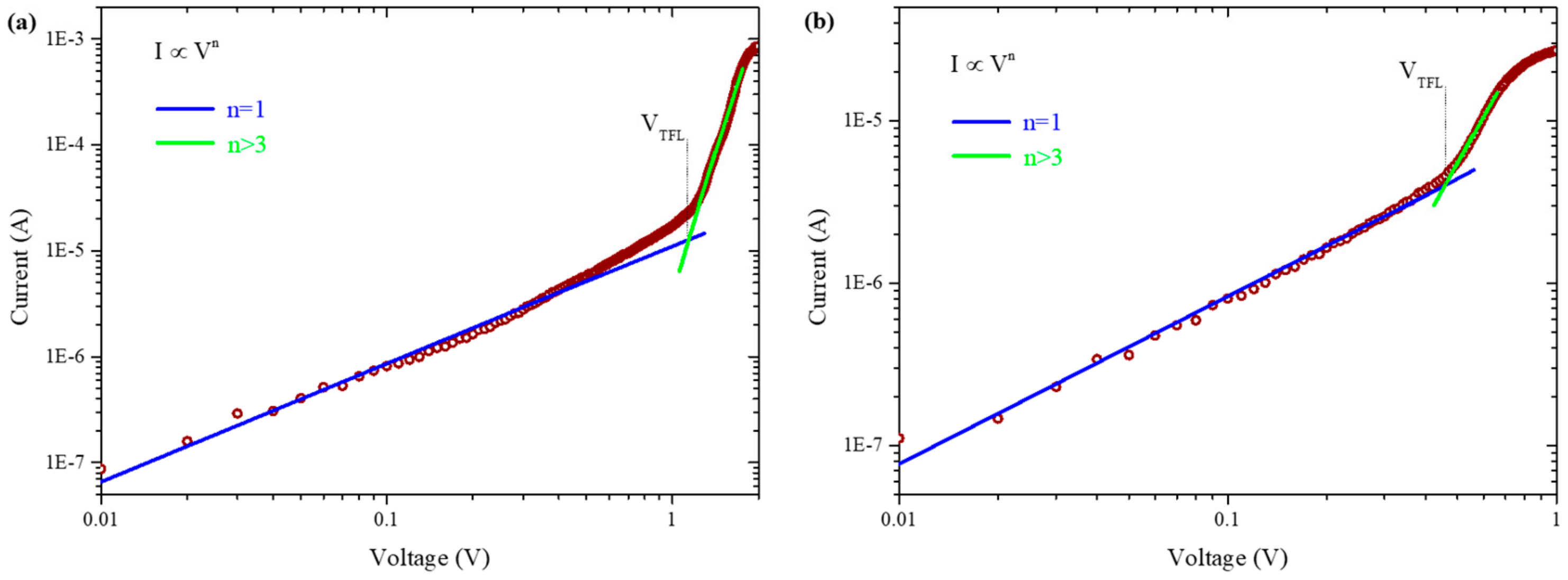
Large grain size and compact CH
3NH
3PbI
3 film tends to yield less trap states, which are beneficial for high-performance PSCs [
8,
29]. Hence, hole trap density in the CH
3NH
3PbI
3 films was quantified by the dark I-V analysis for hole-only devices.
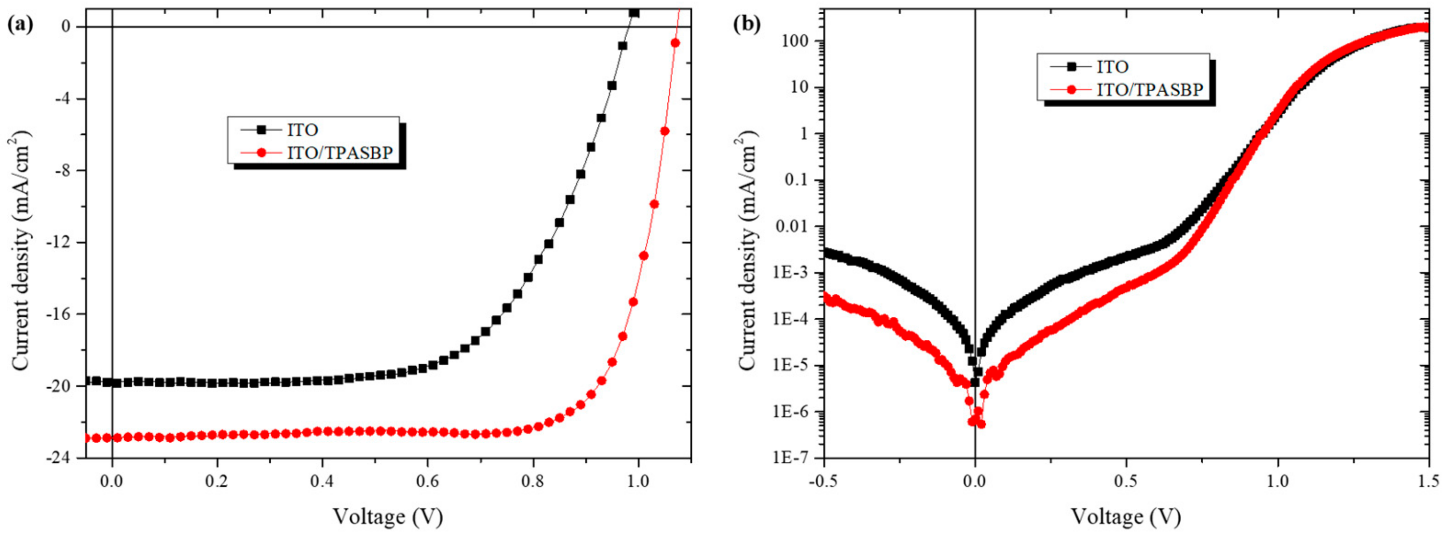
Figure 3a,b show the I-V curves of the hole-only devices based on ITO and ITO/TPASBP substrates in the dark. It is clear that the linear regime (blue line) at low voltage indicates an ohmic response of the hole-only devices. With the increase of voltage, the current exhibits a rapid nonlinear rise (green line), presenting the transition to the trap-filled limit (TFL) regime in which all the available trap states are filled by the injected carriers. The TFL voltage V
TFL is determined by the trap density [
30,
31]:
where e is the elementary charge of the electron, L is the thickness of the CH
3NH
3PbI
3 film, ε is the relative dielectric constant of CH
3NH
3PbI
3 (ε = 30) [
32], ε
0 is the vacuum permittivity, and n
trap is the trap density. The onset voltage V
TFL is linearly proportional to the density of trap states, n
trap; hence, the trap density can be calculated using Equation (1). Based on
Figure 3a,b the V
TFL values for the CH
3NH
3PbI
3 films grown on ITO and TPASBP are 1.12 and 0.46 V, respectively. Correspondingly, the CH
3NH
3PbI
3 film on bare ITO yields a hole trap density of 1.48 × 10
16 cm
−3, whereas the CH
3NH
3PbI
3 film deposited on TPASBP has a hole trap density as low as 6.10 × 10
15 cm
−3.
On the basis of the above results, it was clear that a hydrophobic surface provided by TPASBP was beneficial for the formation of dense pinhole-free CH3NH3PbI3 film with a larger grain size relative to hydrophilic substrates, thus resulting in better crystallization of CH3NH3PbI3. Meanwhile, due to the improvement of CH3NH3PbI3 morphology and crystallization, the trap density was reduced significantly for the perovskite film fabricated on TPASBP compared with that on ITO, which induced less recombination loss in the PSCs.
Besides the hydrophobicity, TPASBP also has high hole mobility because of its linear π-conjugated structure, which has been illustrated before elsewhere [
26,
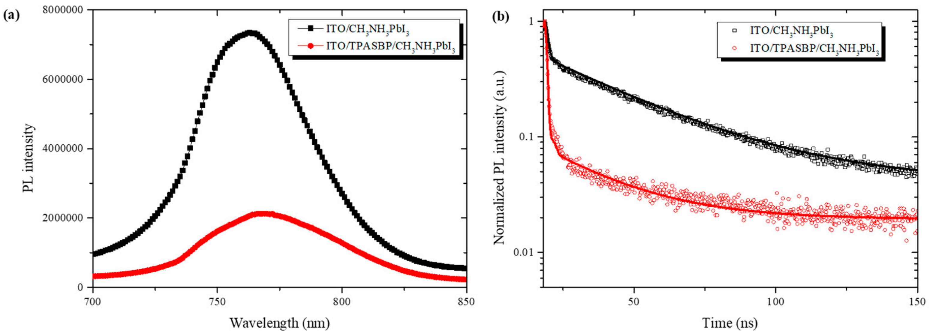
33]. Meanwhile, the results of steady-state PL and time-resolved PL (TRPL) shown in
Figure 4 also revealed that the hole-extraction efficiency at the ITO/CH
3NH
3PbI
3 interface was improved by using TPASBP. As presented in
Figure 4a, a much stronger quenching effect on the PL of the CH
3NH
3PbI
3 film on TPASBP was observed in comparison with that on ITO, suggesting an enhanced hole-extraction ability of TPASBP as an HTM. In order to further evaluate the hole-extraction rate, TRPL was performed and the decay curves are shown in
Figure 4b. By a biexponential fitting of the dynamic TRPL data, the CH
3NH
3PbI
3 film on ITO exhibited a longer lifetime of 32.26 ns, whereas the lifetime of CH
3NH
3PbI
3 film grown on TPASBP was 21.87 ns. More details about carrier lifetime can be found in
Table S1. The smaller PL lifetime of CN
3NH
3PbI
3 fabricated on TPASBP indicates the reduced carrier recombination due to the more efficient hole extraction and transport in CH
3NH
3PbI
3 film. The high mobility and the enhanced hole-extraction ability of TPASBP contributes to the high carrier collection efficiency of PSCs, thus leading to an enhancement of short-circuit current (Jsc).
3.2. Photovoltaic Performance of PSCs
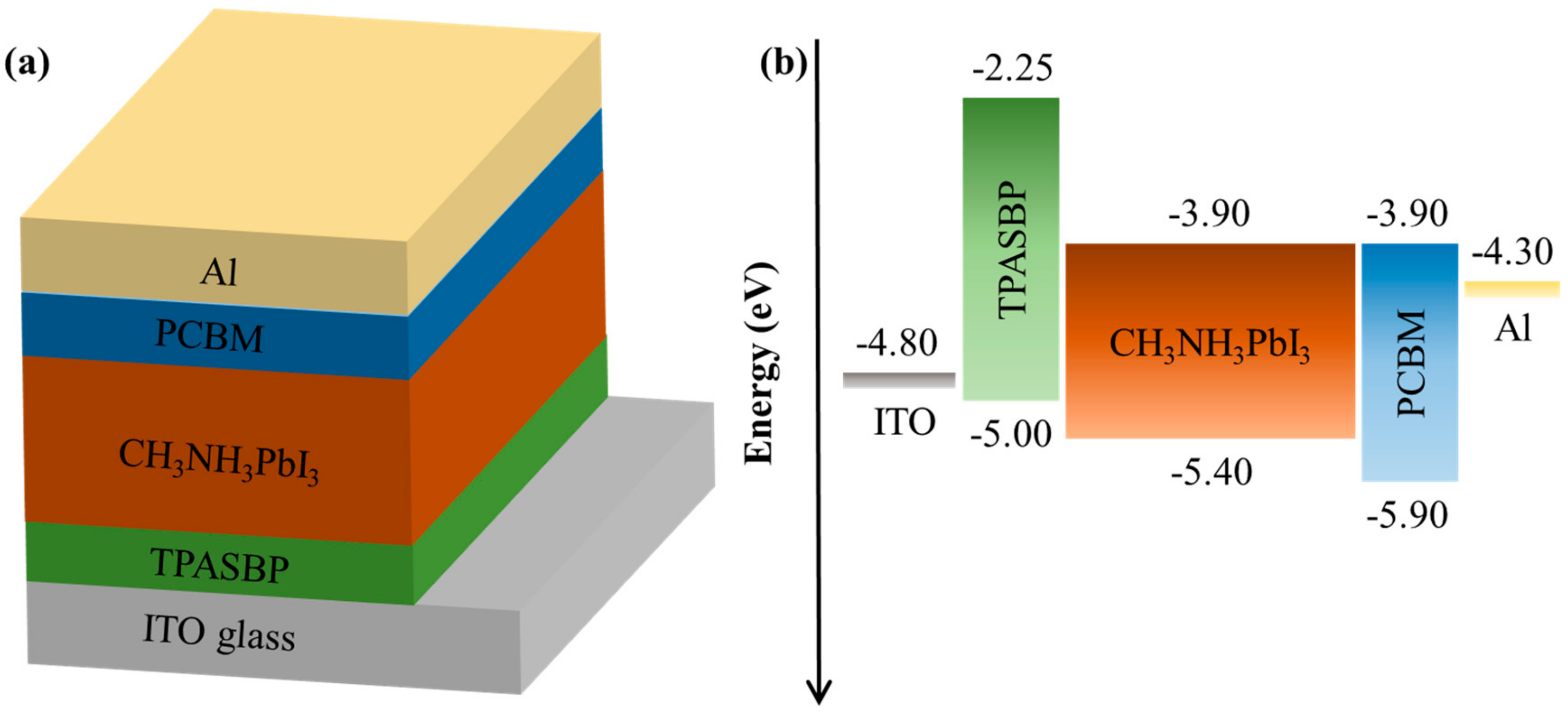
The influence of TPASBP on device performance was evaluated in inverted PSCs with a structure shown in
Figure 5a, in which all layers between the electrodes were fabricated by spin-coating. The relative energy levels are presented in
Figure 5b, where it can be seen that the highest occupied molecular orbital (HOMO) of TPASBP is between the work function of ITO and the valence band (VB) of CH
3NH
3PbI
3, implying that the potential energy loss at the interface of TPASBP/CH
3NH
3PbI
3 can be lowered.
The J-V characteristics of the inverted PSCs fabricated on TPASBP under 100 mW/cm
−2 illumination (AM 1.5 G) are shown in
Figure 6a. The same irradiation was carried out on PSCs based on bare ITO for comparison. PSCs fabricated on TPASBP afforded the best PCE of 18.72% with a Jsc of 22.87 mA/cm
−2, an open circuit voltage (Voc) of 1.07 V, and a fill factor (FF) of 76.47% (listed in
Table 1). The histogram of PCE shown in
Figure S5 also indicates that inverted PSCs based on TPASBP exhibit good reproducibility, with an average efficiency of 17.23%. Meanwhile, the dependence of PSCs performance on the thickness of TPASBP is plotted in
Figure S6, which reveals a thickness of 20 nm is optimal for TPASBP.
Dark J-V characteristics shown in
Figure 6b indicates that the leakage current density at the low voltage scale was weakened dramatically in the PSCs with perovskite film grown on TPASBP. It has been reported that the leakage current is determined by R
Sh and consequent charge carrier recombination [
34]. A reduction of leakage current means an increase of R
Sh and a reduction of charge carrier recombination in the device. The result of dark J-V was in good agreement with that of the reverse saturation current, which is discussed in the following part, revealing the remarkable role of TPASBP in preventing recombination in PSCs.
The improved FF and Voc strongly imply a reduction in recombination loss as a result of the utilization of TPASBP in inverted PSCs. The planar structured PSCs can be treated as single heterojunction diode. The electric parameters of the PSCs, including series resistance (Rs), and reverse saturation current density (J
0), can be extracted from the J-V curves shown in
Figure 6a according to the diode equation [
35,
36]:
where A is the ideality factor of the heterojunction, and K
B and T are the Boltzmann constant and absolute temperature, respectively. Equation (2) can also be written as (where R
Sh is large enough):
The calculated values of A, Rs, J
0 are listed in
Table 2. For a well-behaved heterojunction solar cell, the ideality factor is typically in the range of 1.3 ˂ A ˂ 2 [
36]. In the PSCs with perovskite film grown on TPASBP, the ideality factors obtained from Equations (3) and (4) are 1.56 and 1.72, respectively, which indicate that the PSCs based on TPASBP work well on the basis of a heterojunction model. It is also clear that Rs is much lower in the PSCs fabricated on TPASBP (1.19 Ω cm
2) than the PSCs fabricated on ITO (5.68 Ω cm
2). As also shown in
Table 2, J
0 for the PSCs with perovskite film grown on TPASBP is ∼2 orders of magnitude lower than those PSCs on ITO. J
0 correlates with the carrier recombination in heterojunction solar cells, where a lower J
0 corresponds to lower carrier recombination in PSCs. Therefore, the recombination in inverted PSCs is greatly lowered by using TPASBP. Meanwhile, according to the equation Voc = (AK
BT/e)ln(Jsc/J
0+1), smaller J
0 also leads to larger Voc; hence, Voc in the PSCs with perovskite film deposited on TPASBP is higher than that on ITO.
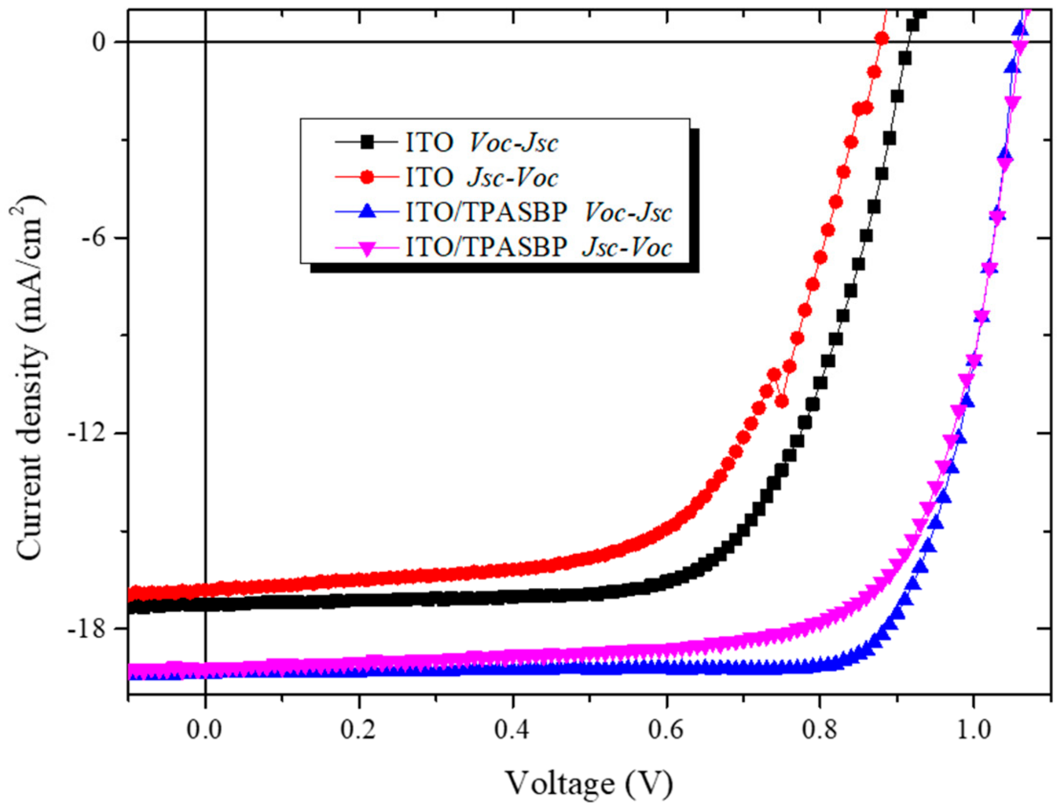
Finally, the hysteresis of these devices was investigated, as displayed in
Figure 7. According to the device performance of PSCs with respect to the scan direction under a 10 mv per point (voltage scan step) condition, it was clear that the PSCs based on ITO had much more serious J-V hysteresis while the PSCs fabricated on TPASBP gave almost the same values of Voc and Jsc with a small difference of FF under different scan modes. The restrain of hysteresis by TPASBP can be attributed to the improved quality of the CH
3NH
3PbI
3 film and the significant decrease of recombination in the devices, which derived from the pinhole-free morphology and lower trap density of CH
3NH
3PbI
3 grown on hydrophobic TPASBP, as described above.


