3.1. Sample Characterization with Raman and X-ray Photoelectron Spectroscopy
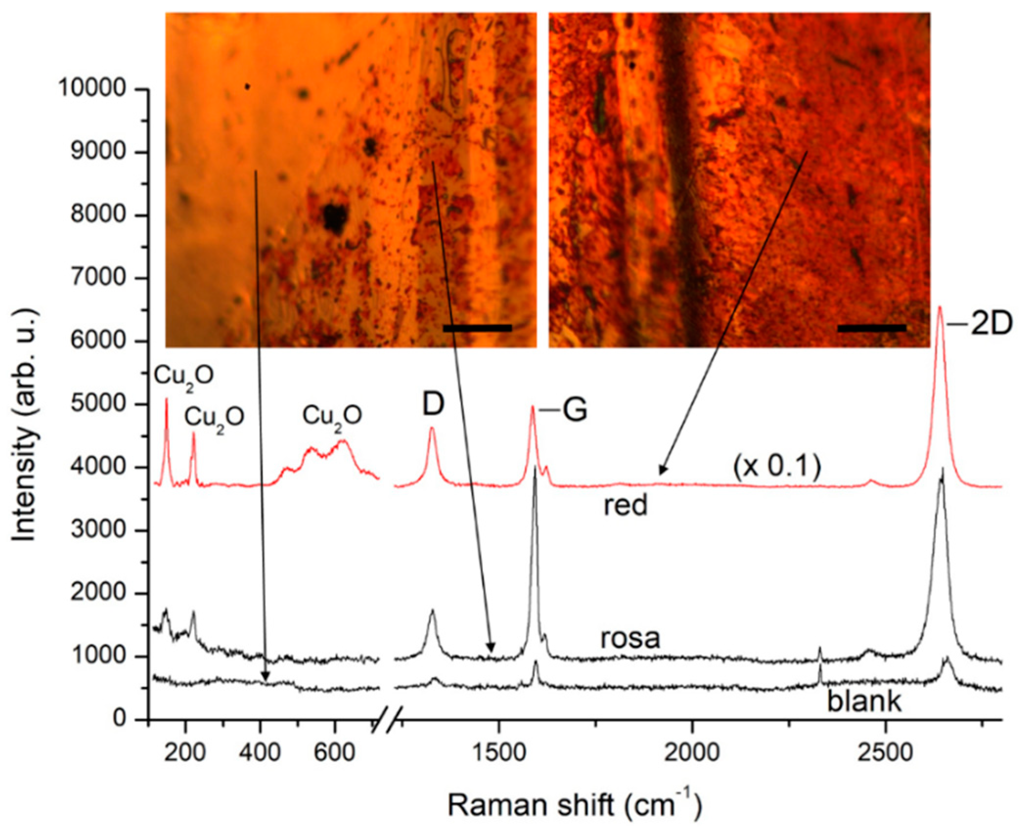
A typical case of time evolution of a graphene-coated Cu (Gr/Cu) foil is depicted in
Figure 1. After prolonged storage at ambient conditions (typically longer than 6 months) the Gr/Cu foil exhibits regions with different color contrast under the optical microscope as seen from the two microscopic images in
Figure 1. The difference in color contrast implies different oxidation degrees, with yellow color indicating blank copper, pale-red (or rosa) color indicating slight oxidation, and the redder tones indicating a more heavily oxidized state (Cu
2O). When freshly taken out of the CVD chamber, the entire area of the foil looks similar to the left part of the left image with corresponding typical Raman spectrum as the “blank”-marked trace in
Figure 1. The color changes visibly in the right part as well as in the whole right image are very nonuniform, indicating that some parts of the Gr/Cu surface are more resilient to oxidation than others. The Raman spectra also confirm the difference in the oxidation degrees with the “red”-marked spectrum displaying more than 10 times more intensive Cu
2O bands at 149, 216, 525 and 640 cm
−1 [
21] than the “rosa”-marked one. On the other hand, the complete lack of such bands in the “blank”-marked spectrum and the clean yellow surface of the grain encompassing the left part of the left image in
Figure 1 show that graphene has largely preserved this grain from oxidation. The Raman features of graphene in
Figure 1 suggest that it is strongly coupled to Cu in the seemingly nonoxidized blank areas (low intensity and large blue shift of the G and 2D band [
15]) while over the red areas this coupling is largely released and the corresponding Raman features change towards those of free-standing graphene.
To obtain a more quantitative picture of the oxidation development with time we performed a detailed characterization with different experimental methods on 3 samples with different storage times after CVD growth (6 months for the second and 20 months for the third sample) and with consecutive increasing density of reddish coloring. These samples will be referred to as “6 months” and “20 months” in what follows. The first sample referred to as “fresh” was examined immediately after graphene growth.
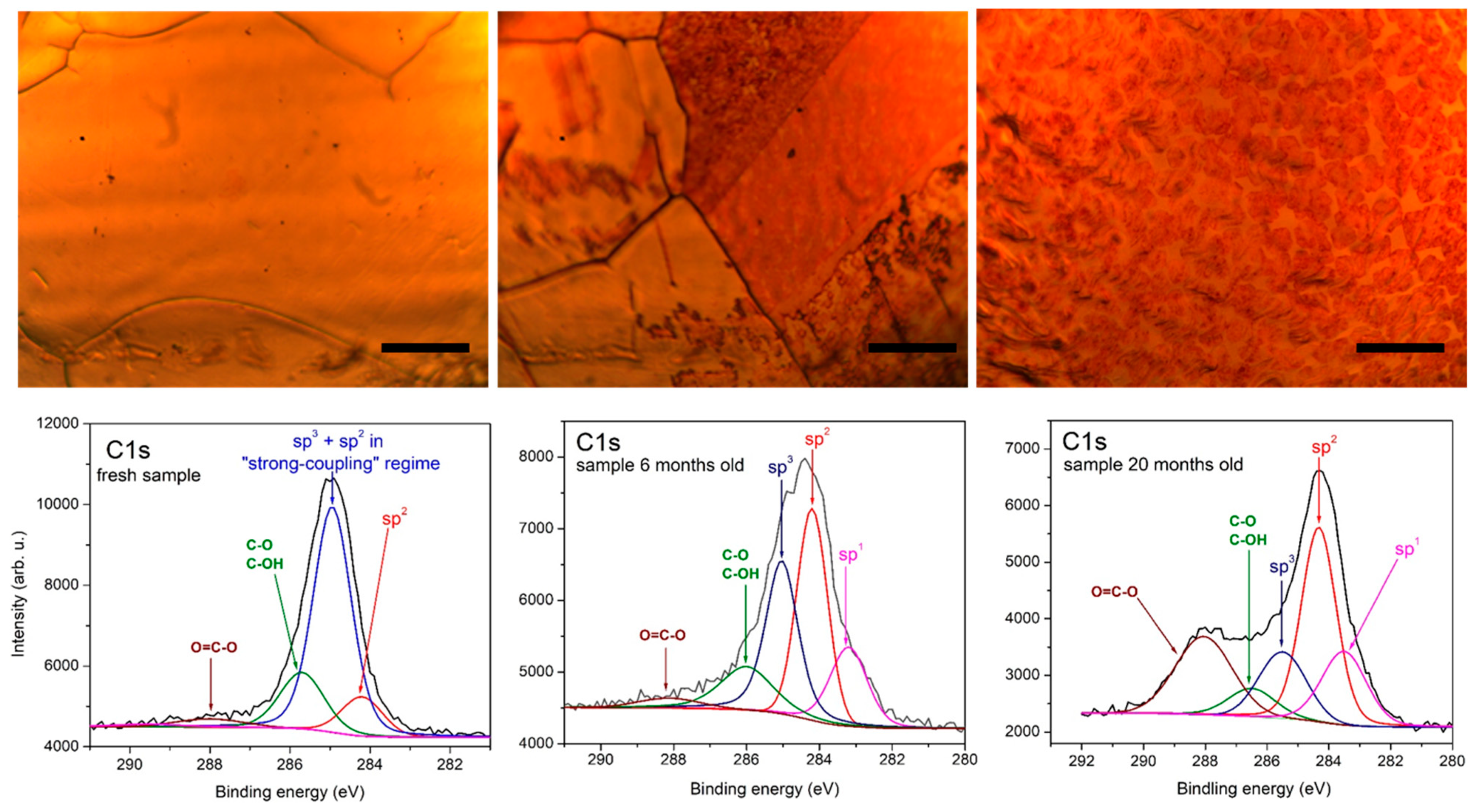
A detailed XPS examination of the three samples was performed. Microscopic images and fitted C1s spectral bands are displayed in
Figure 2.
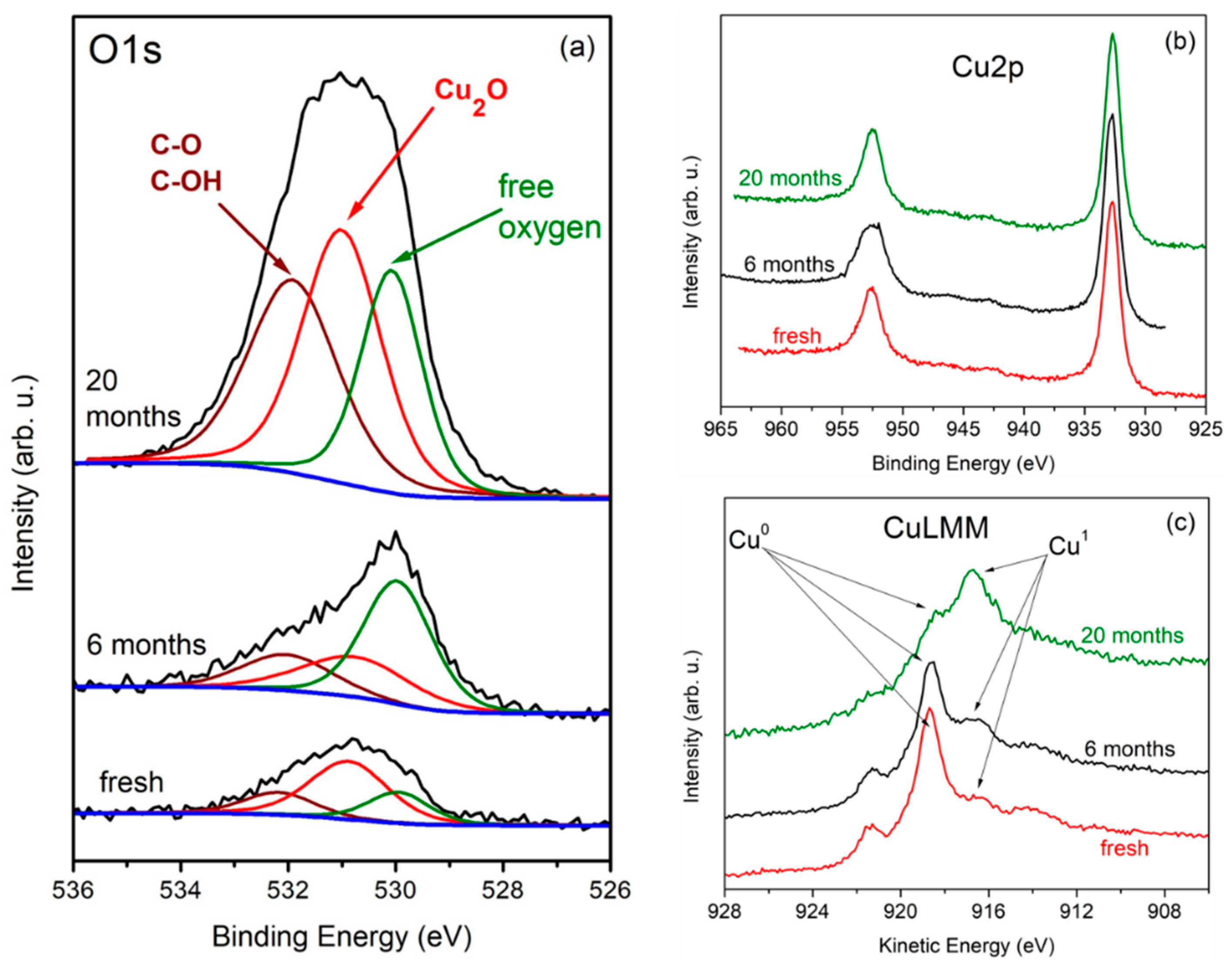
Figure 3 shows Cu LMM Auger spectra, Cu 2p spectra and O1s spectra for the three samples.
The C1s spectra are complex and their most intense component is typically the C1s peak of sp
2 graphene at 284.2–284.4 eV. Interestingly, only for the “fresh” sample there is a peak at around 284.9 eV with much higher intensity than that of the conventional sp
2 peak. This is consistent with the assumption that immediately after the growth process, the major part of the graphene layer is still strongly coupled to the copper substrate via exchange interactions between the Cu valence electrons and the carbon C1s core hole which yields a C1s sp
2 signal at 284.75 eV [
22]. In our case, this “strong-coupling” peak is slightly upshifted due to contributions from sp
3 sites as well as defects in the graphene honeycomb lattice and C-H bonds whose signal is located between 285.0 and 285.5 eV. In the C1s spectra of the other samples these three contributions form a separate peak which is denoted as sp
3 peak. Several other satellite peaks due to oxygen-containing groups are also detected. The peak at around 286 eV belongs to C-O/C-OH moieties, that around 288 eV to O=C-O bonds and carbonate groups, and that at ≈283 eV to sp
1 type carbon bond in C
2Cu. As expected, the oxygen-related peaks are more intense for longer storage time.
The O1s photoelectron spectra are also complex and were fitted with three peaks (see
Figure 3a). According to the literature, the peak at the lower binding energy side at ~529.8 eV corresponds to an atomic phase state, i.e., a low-bound state [
22,
23,
24,
25] showing that there is a certain amount of free oxygen trapped by the graphene layer which serves as a reservoir for further Cu oxidation [
26]. The middle peak at ~530.7 eV corresponds to Cu
2O. As expected, this oxidation-related peak has maximum intensity for the sample with the longest storage time of 20 months. There is a shoulder at the higher binding energy side which is accounted for by the third peak at around 532 eV. The appearance of this shoulder is related to formation of C-O/C-OH and C=O bonds. From the Cu 2p photoelectron spectra in
Figure 3b it is also obvious that the copper substrate is oxidized. The chemical states of copper were found to be Cu
0 (Cu metal) and Cu
1+ (Cu
2O) for all studied samples. The same is evidenced by the Auger CuLMM line (see
Figure 3c) where the oxidation-related peak gains intensity with increasing storage time.
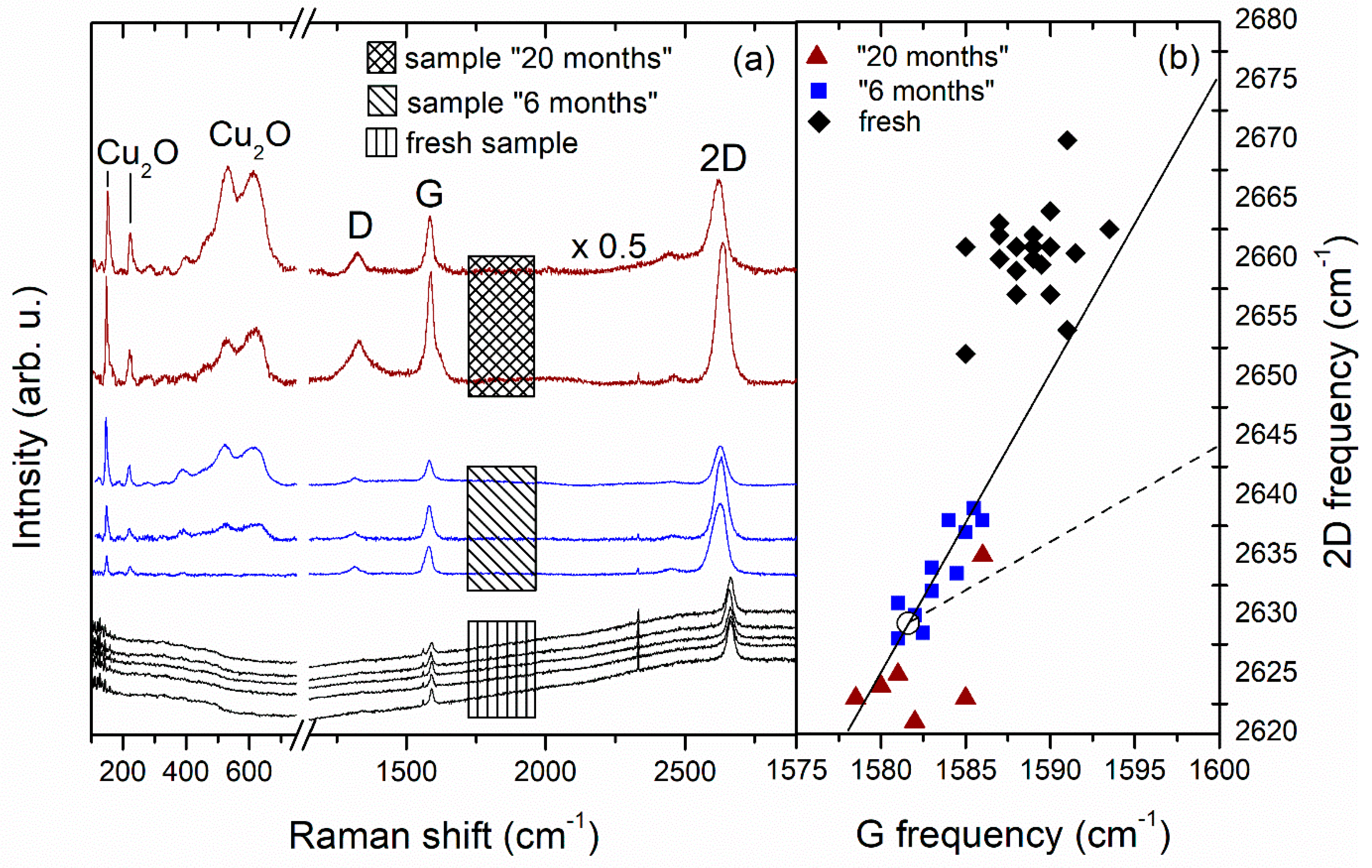
Comprehensive spatially resolved Raman measurements were performed on the three samples. Representative spectra from this characterization are presented in
Figure 4a. Recently it was shown for graphene grown on Cu that in ω
G-ω
2D space the correlative shift of ω
G and ω
2D can be decomposed into a purely strain-induced shift [
12] and a shift due to the fractional change in the effective Fermi velocity provided the graphene layers are do**-free [
27]. As there is increasing evidence in the literature that the do** of graphene on Cu foil is negligible and thermally activated [
28,
29], we can apply a similar approach and show in
Figure 4b the (ω
G, ω
2D) values from our measurements on the three samples. As can be appreciated from
Figure 4a,b, the entire surface of the “fresh” sample displays a low-intensity graphene signal characteristic for strong coupling to the Cu substrate, with typical frequency values grou** around 1589 cm
−1 for ω
G and around 2660 cm
−1 for ω
2D. This indicates significant compressive strain and, on the other hand, ω
2D is additionally upshifted due to the Fermi velocity reduction which is significant for our low excitation laser energy of 1.96 eV [
27]. As the spectra of sample “6 months” were taken mostly from reddish-colored grains, there is a characteristic gathering of its (ω
G, ω
2D) values around the zero-strain point at (1581.6, 2629.3) cm
−1 [
27] with some points still indicating residual compressive strain. The Cu
2O bands, which are completely missing in the “fresh”-sample spectra, display considerable intensity in the spectra of the two older samples. The (ω
G, ω
2D) values for sample “20 months” are more scattered with some points implying a transition to tensile strain imposed by local Cu
2O aggregations [
27]. It should, however, be pointed out that the strain release in the graphene lattice takes place in a very nonuniform way and there are still some isolated Cu grains in sample “6 months” which have preserved their initial “bare-copper” color and yield Raman spectra reminiscent of the strong-coupling regime.
From the collected Raman data, we obtained values for the peak intensity ratio of the 2D and G band I(2D)/ I(G) ranging from 2 to 2.8 which can, however, be impacted by the graphene-Cu coupling. In the
Supporting Information we report a comprehensive Raman characterization of part of the “fresh” sample after transfer on glass substrate. As can be seen from
Figure S1, I(2D)/ I(G) values obtained from this characterization range from 2.6 to 3.2 with a mean value of 2.9. The 2D bandwidth (FWHM) has a narrow distribution with mean value 30.8 cm
−1 (compared to ~29 cm
−1 before transfer). In
Figure S2 we show scanning electron microscopy (SEM) images from the “fresh” sample and sample “6 months” displaying predominantly uniform brightness with occasional small regions of darker contrast. We interpret the combined Raman and SEM results as an indication for mainly single-layered graphene with possible minor presence of randomly stacked bilayer islands.
The oxygen content in the 3 examined samples as calculated from the XPS spectra is given in
Table 1. Considering the XPS response of samples “6 months” and “20 months” shown in
Figure 2 and
Figure 3, it is noticeable that the increased presence of oxygen affects not only the Cu surface but also the graphene layer itself through various etching reactions. On the other hand, the D band intensity in the Raman spectra in
Figure 1 and
Figure 4 increases much stronger than that of the G and the 2D band in going from seemingly nonoxidized (blank) to highly oxidized (red) spots. This indicates that, with time, the defect density of the graphene coating of a certain copper grain becomes an important factor for formation and gradual enlargement of Cu
2O patches on this grain. Still, we regard oxygen etching of graphene edges and grain boundaries as the main mechanism ensuring a slowly advancing oxidation of the substrate [
9]. As was shown in [
22], vacuum annealing at 700 °C can restore the strong graphene coupling to the Cu substrate. We expect that annealing in vacuum or inert atmosphere [
30] at even higher temperatures approaching the CVD growth ones may help reducing the trap states in such “aged” graphene or recover its lattice ordering where it is locally deteriorated by oxygen-related etching reactions. The surface orientation of the Cu grain is another key factor for its oxidation rate and will be discussed in what follows.
3.2. Study of the Cu Surface Oxidation with Ellipsometry and Electron Backscattering Diffraction (EBSD)
To examine the weakening of the Cu-graphene coupling upon oxygen intercalation it is instructive to find a measure for the separation of the graphene layer from the Cu surface. We therefore estimated the thickness of the formed Cu
2O layer by means of spectroscopic ellipsometry (SE) for the fresh and the 6-month-old sample. There are only few ellipsometric studies of as grown graphene on metals [
31], while most of them are carried out on transferred graphene [
32,
33].
As there is increasing evidence that the Cu oxidation rate beneath the graphene depends on the surface orientation of the copper grains [
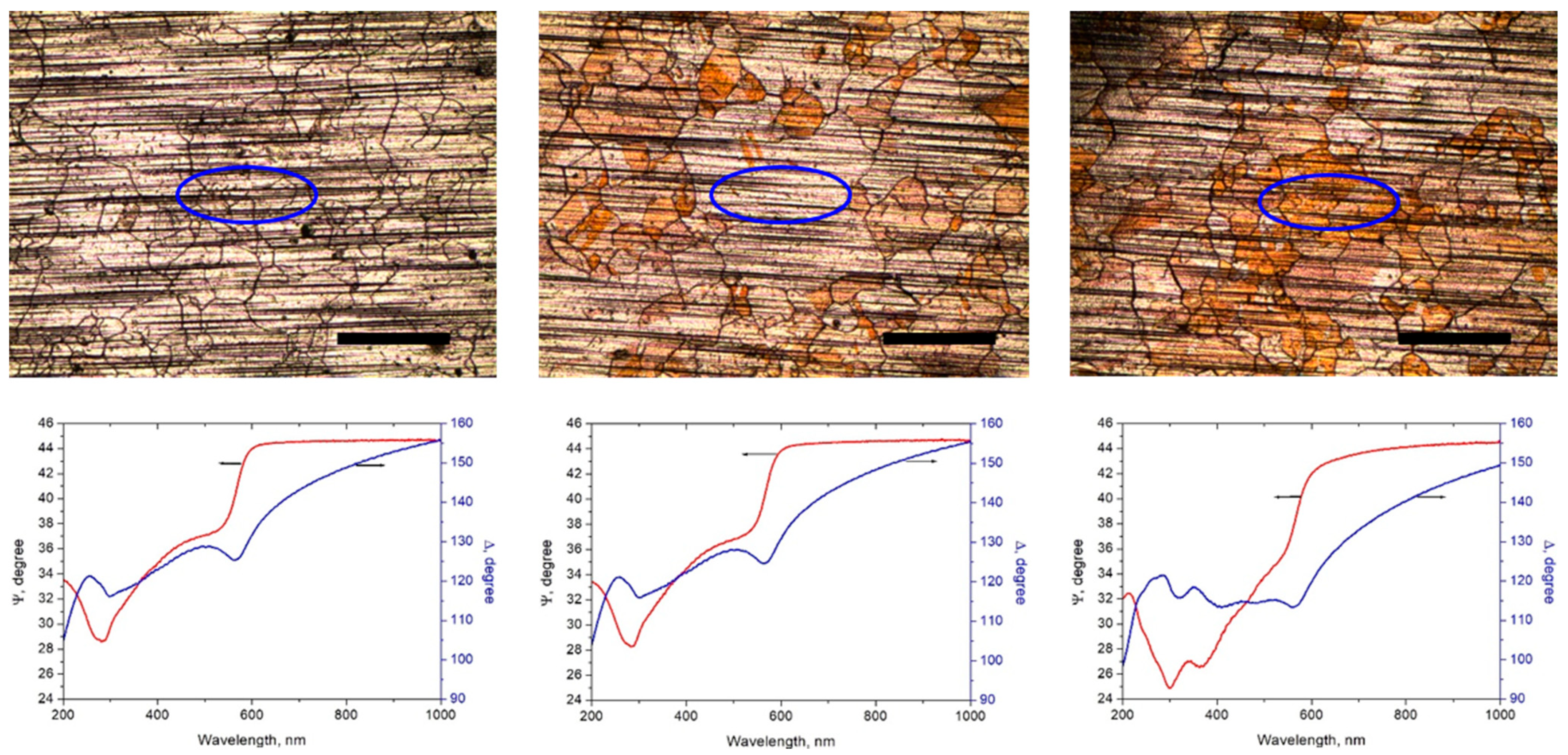
17], we examined two regions from sample “6 months”—one with predominant reddish color and one with apparently low oxidation degree. The regions from which the SE signal was collected, are shown in
Figure 5 along with the corresponding dispersion spectra for the ellipsometric quantities Ψ and Δ.
The ellipsometric data for Ψ and Δ were modelled within a model consisting of two consecutive layers on top of an oblique substrate which is the copper foil. The first layer is Cu
2O participating in the model with optical constants taken from Palik’s Handbook of Optical Constants [
34] (CompleteEASE software). The second (top) layer is graphene with optical constants of graphite, taken again from [
34]. The graphene layer thickness was assumed to be 0.35 nm as the combined Raman and SEM results indicate predominant monolayer graphene. Using this model, the following Cu
2O average thicknesses were obtained: fresh sample: ≈0 nm; sample “6 months” low-oxidation region—0.5 nm; and sample “6 months” high-oxidation region—6.5 nm. From the strong variation of the oxide thickness and the obvious coincidence of the boundaries of differently colored regions with the Cu grain boundaries, as can be appreciated from the microphotographs in
Figure 3 and
Figure 5, it is obvious that the crystallographic orientation of the Cu surface has a key influence on the rate and degree of its oxidation.
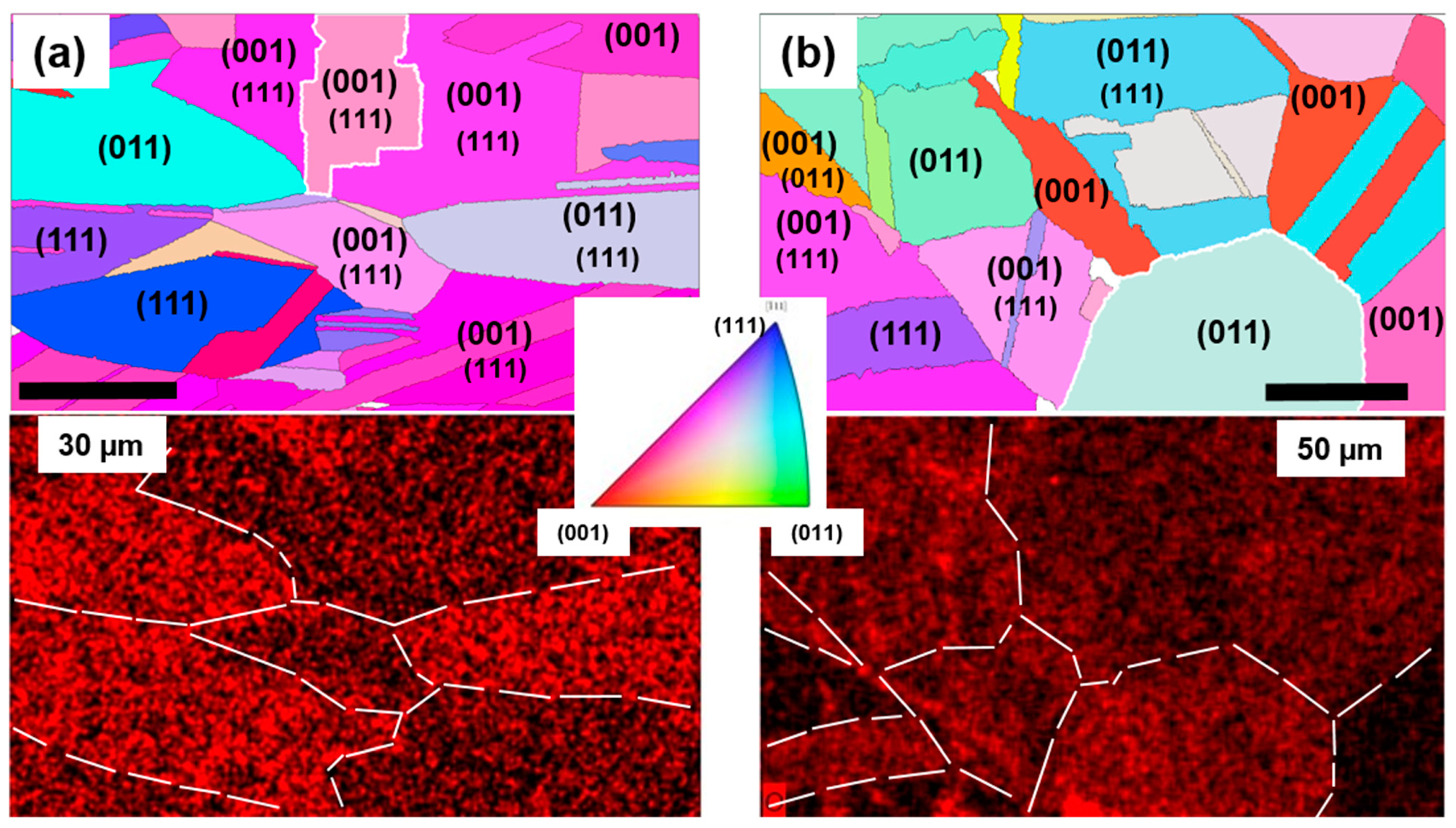
To check this influence in detail, we examined the “fresh” sample and “6 months” sample by the EBSD technique. This study was conducted 2 months later in order to have initial Cu oxidation in the “fresh” sample. As this method has an effective probing depth above 10 nm, it can be safely assumed that the graphene and the oxide layer do not mimic the EBSD signal, which is almost entirely collected from the underlying copper [
17]. Cu surface orientation maps were obtained by EBSD and, simultaneously, oxygen elemental distribution maps were measured by energy-dispersive X-ray spectroscopy (EDX) on the same spots in order to correlate the Cu orientation to the Cu
2O content. The results were presented using the MTEX Matlab toolbox [
35].
Figure 6 shows EBSD and EDX results for the “fresh” sample and “6 months” sample. As can be expected for a polycrystalline Cu foil, the majority of the grains are not perfectly oriented according to the basic Miller indices of the m3m structure. However, from the depicted orientation maps, it is noticeable that in both graphene-coated samples, predominantly (011) oriented Cu grains are most susceptible to Cu
2O formation while grains with dominant (001) orientation exhibit the lowest oxidation rate. Grains with orientation near to (111) display an intermediate affinity towards oxidation. Surprisingly, these results are the opposite to those reported in [
17], where for graphene-coated Cu foils the (001) grains were found to be most susceptible to oxidation and (011) grains most resilient to it. A possible explanation for this contradiction may lie in different substrate pretreatment and different details in the growth recipe. Our foil substrates were electropolished while those used in [
11] were annealed in air at 250 °C prior to the CVD growth process. Under the preparation conditions applied in this study, rippling of the Cu surface and formation of terrace step bunches, while occasionally present, could be avoided to a large extent. As was shown by Hu et al. [
36], the parameters of the initial stages of the CVD prior to the growth stage itself can significantly influence the physical properties of the Cu substrate. Moreover, a heat-treatment experiment performed by Wood et al. [
9] on polycrystalline Cu foils with graphene revealed that (011) grains are the first among low-index grains to succumb to oxidation when heated. In
Figure S3 of the Supporting Information we present EBSD results on two other Gr/Cu foil samples which confirm the observed dependence of the oxidation rate on the Cu grain surface orientation.
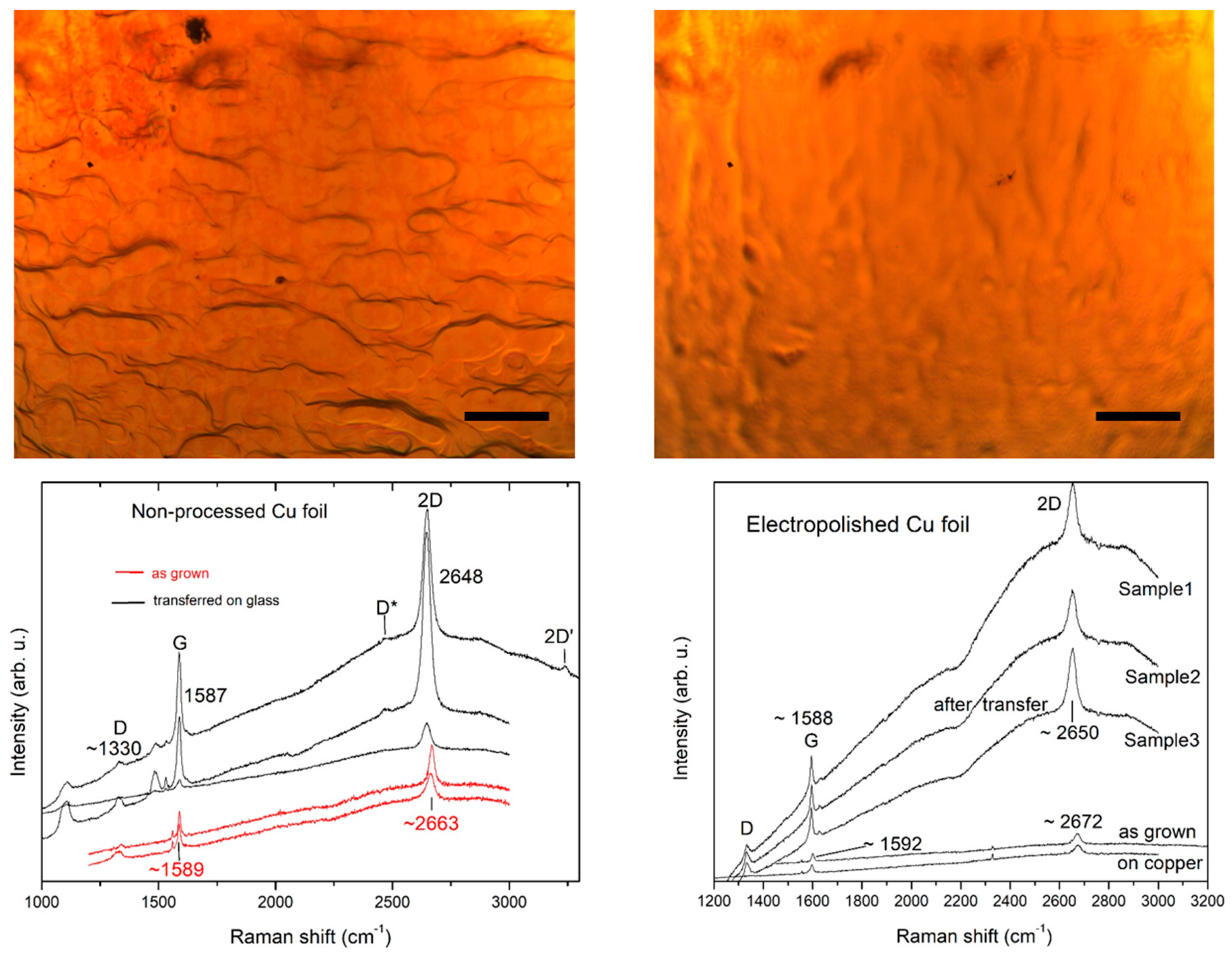
3.3. Examination of the Effects of Electropolishing
Electropolishing has been frequently applied as part of the Cu foil pretreatment to lower its surface roughness and to achieve better quality of the grown graphene [
37,
38]. Here, we compare the characteristics of graphene grown on Cu foil electropolished prior to the CVD growth and on Cu foil that has not undergone such pretreatment. The results from monitoring with optical microscopy and Raman spectroscopy are depicted in
Figure 7. It is seen from a comparison of the microscopic images that the electropolished foil exhibits a better resistance to Cu oxidation, while the unprocessed Gr/Cu foil shows precursors of pale-red coloring already 1 week after the graphene growth process.
From the Raman spectra in
Figure 7, it is seen that graphene grown on electropolished Cu foil experiences a stronger coupling to the Cu substrate and a stronger strain (2D band redshift of more than 20 cm
−1 after transfer onto glass as compared to ~15 cm
−1 for unprocessed Cu foil). It is also found that the Cu-graphene coupling makes the intensity ratio of the 2D and G band less informative for determination of the number of layers and it becomes a reliable parameter only after the transfer on isolating substrate.
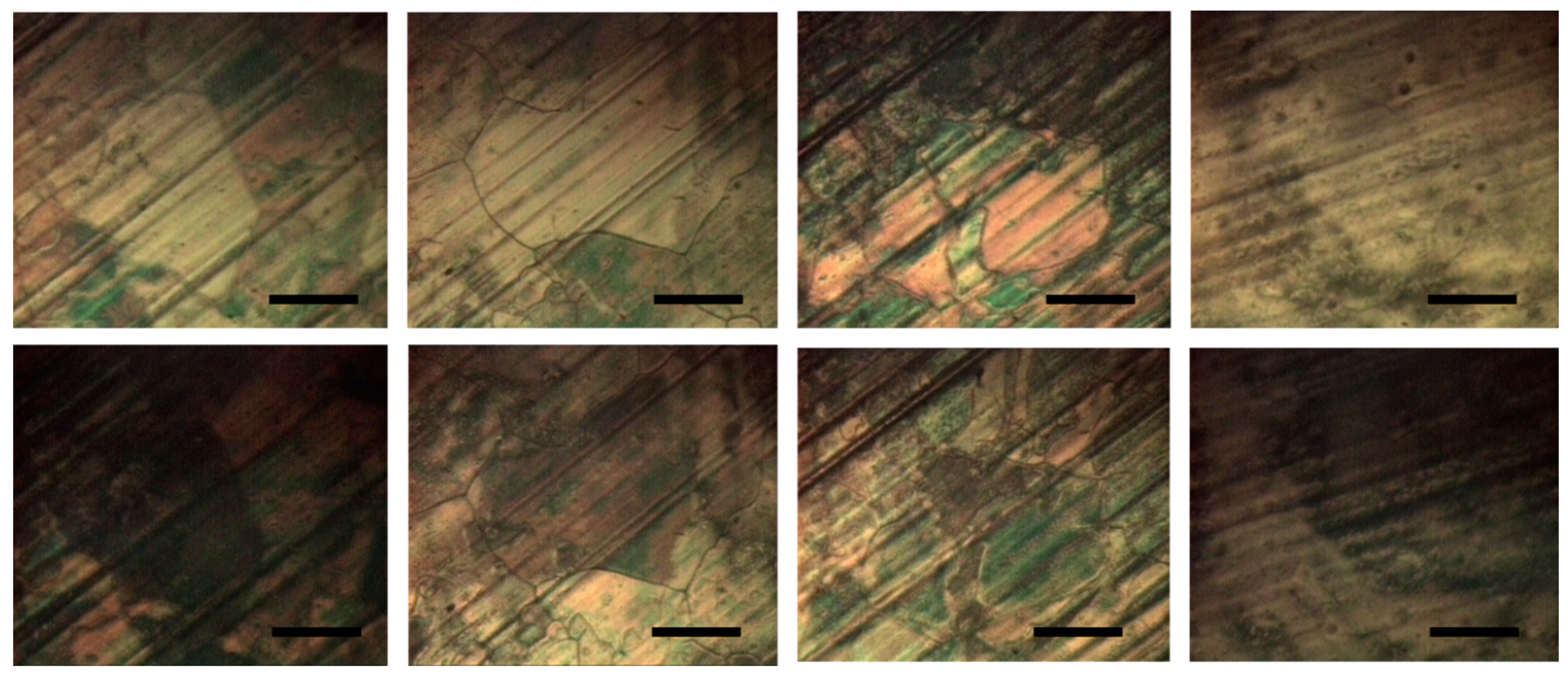
To further illustrate the effect of electropolishing, we visualize the domains in the graphene layers grown on an electropolished and on a nonprocessed Cu foil by means of the nematic liquid crystal (LC) E7. This is possible due to the interaction of two-dimensional graphene-honeycomb structure with the LC benzene rings through π–π electron stacking (binding energy of −2eV) which induces a planar alignment of the LC, thus creating LC pseudonematic domains (PNDs) at the graphene surface [
39]. As the graphene layer consists of grains with different crystallographic orientation and each grain imposes its own ordering on the LC, the shapes and boundaries of these anisotropic LC domains strongly correlate with those of the graphene grains. When observed through a reflected cross-polarized microscope, such PNDs with homogeneous planar alignment transit from a bright to a dark state upon rotation at 45° [
39]. Distinct graphene grains can thus be visualized [
39] and observed simultaneously with the copper grains.
Figure 8 shows pairs of such microphotographs taken from E7-coated graphene grown on electropolished and nonprocessed Cu foil. As is seen, the PNDs formed on electropolished Cu foil (
Figure 8, left two pairs) are large and well outlined with clear boundary walls suggesting that the LC has achieved a uniform planar orientation. This indicates a high crystalline quality of the underlying graphene which is an important prerequisite for the above described π–π stacking mechanism. Thus, larger graphene grains are found on electropolished Cu foil which can overgrow Cu grain boundaries presumably due to the smaller Cu surface roughness. On the other hand, the PNDs in the right two image pairs in
Figure 8 (nonprocessed Cu foil) display enhanced birefringence (recognized by the red coloring) and unclear boundaries which are signs for nonuniform and deteriorated planar alignment. We attribute this to the smaller graphene grains with higher defect density on the nonprocessed Cu foil, which cannot achieve an efficient π–π stacking interaction with the LC. Indeed, the Raman spectra of graphene on electropolished foil in
Figure 7 completely lack a D band compared to the well-discernible D bands in the spectra from the nonprocessed foil.


 and
and 


