1. Introduction
Two-dimensional (2D) layered materials have always been a cutting-edge field in condensed matter physics and materials research [
1]. Various 2D layers can be combined using van der Waals (vdW) forces to build heterostructures with diverse functionalities [
2]. These heterostructures exhibit a range of excellent properties and are applied to optoelectronic devices [
3], providing unprecedented opportunities for the development of advanced nanoelectronics devices [
4].
As one of the atomically thin 2D materials, graphene [
5] has attracted worldwide attention due to its excellent optical [
6], electrical [
7], and mechanical properties [
8], and it is expected to be used to build a new generation of miniaturized and intelligent electronic devices [
9]. However, the absence of a band gap has limited the application of graphene, particularly in the semiconductor industry [
10]. Significant efforts have been devoted to addressing this issue in the gap-opening of graphene, like functionalization [
11], do** [
12], and the construction of heterostructures [
13]. Recently, many graphene-based vdW heterostructures have been investigated theoretically and experimentally [
14]. For instance, Lan et al. transferred graphene grown on a copper foil to a sapphire substrate with Bi
2Te
3 crystals via low-pressure chemical vapor deposition (CVD). The crystallized Bi
2Te
3 was synthesized directly using spin-coated coring (SCCA). This procedure avoided any degradation of the nanoplates and significantly improved the quality of the heterojunction sample [
15]. Hu et al. utilized a polymethyl methacrylate (PMMA)/polydimethylsiloxane (PDMS) blend to transfer metal-catalyzed CVD-fabricated graphene/SiNWS heterojunctions onto stretchable polytetrafluoroethylene (PTFE) substrates. The high preparation efficiency and outstanding quality were extremely encouraging for daily industrial production and life [
16]. Ren et al. developed a novel flexible self-powered photodetector that transfers electrons through a solid electrolyte. The developed flexible WS
2/graphene photodetector displayed a quick photo response time and high photosensitivity [
17]. Liu et al. fabricated Bi
2Se
3/graphene heterojunctions using molecular beam epitaxy and observed a spiral growth mechanism during the growth process [
18]. By vertically stacking single-layer MoS
2/h-BN/graphene, Lee’s team created random access memory with tunneling. It had excellent stretchability, long retention times, and highly dependable memory performance [
19]. Additionally, Liu et al. investigated different conceivable atomic configurations of phosphorene/graphene in-plane heterojunctions and their effects on interfacial heat conductivity by using density functional theory calculations and molecular dynamics simulations [
20]. Gao et al. simulated the heat transfer properties of graphene/MoS
2 heterojunctions using nonequilibrium molecular dynamics simulations and found that the degree of lattice matching of graphene and MoS
2 had an effect on phonon thermal transport [
21]. However, the majority of these studies on graphene heterojunctions primarily focused on their electronic structures [
22], preparation methods [
23], and applications [
24]. Little research has been conducted on their electron transport properties and intrinsic mechanisms.
In this context, constructing new graphene heterojunctions and studying their electron transport properties are essential if one wants to realize the practical application of graphene heterojunctions in nanoelectronic devices. With excellent electron mobility and a large direct band gap, monolayer WS
2 has a lot of potential uses in nanodevices [
25]. In particular, in recent years, there have been significant breakthroughs in its synthesis and applications. For example, Prof. Feng’s group produced monolayer triangular WS
2 single crystal wafers with excellent uniformity, large size, and high quality by controlling the nucleation density by changing the time of the introduction of the sulfur precursor and the distance between the tungsten source and the growth substrate [
26]. Furthermore, some researchers have used chemical do** to significantly improve the optoelectronic performance of WS
2 field-effect transistors [
27]. Inspired by these advancements, we selected monolayer WS
2 to create a series of graphene/WS
2 heterojunction models and design nanoelectronic devices. We systematically investigated their electronic structures and transport properties using first-principles methods based on the density functional theory (DFT) and nonequilibrium Green’s function (NEGF) [
28].
2. Results and Discussions
The hexagonal unit cell of WS
2 was the same as that of graphene. For graphene and WS
2, the optimized lattice parameters were 2.45 Å and 3.15 Å, respectively. The unit cell parameters we calculated closely matched experimental results [
29,
30].
To construct the graphene/WS2 heterojunctions, we used a 3 × 3 × 1 supercell of WS2 and a 4 × 4 × 1 supercell of graphene with 68 total atom numbers, and a 4 × 4 × 1 supercell of WS2 and a 5 × 5 × 1 supercell of graphene with 109 total atom numbers. In this orientation, both components maintained their original hexagonal lattices without surface rotation and exhibited slight lattice mismatches of 3.1% and 2.4%, respectively. The interlayer spacings of the equilibrium geometries of these two heterojunctions were 3.41 Å and 3.46 Å, respectively, which are typical distances in graphene-based vdW heterostructures with weak interactions.
However, the devices built from the above two heterojunctions contained 366 and 603 atoms, separately. Due to the limitations of quantum-mechanics-based calculations used in this study, we continued to construct a series of heterojunctions with specific rotation angles between each surface to reduce the models’ sizes. In these heterojunctions, the interatomic distances were consistently around 3.4 Å, indicating weak vdW interactions. At the same time, we could also analyze the electron transport properties of devices that had different rotation angles. The equilibrium geometries of heterojunctions and their related parameters are shown in
Figure 1 and
Table 1.
In order to prove the thermodynamic stability of these heterojunctions, the binding energies of the graphene/WS
2 vdW heterojunctions were calculated to assess the system stability, as follows:
where
E(heterojunction),
E(graphene), and
E(WS
2) represent the total energy of the heterojunctions, graphene layers, and WS
2 layers, respectively. The calculated binding energies are presented in
Table 2. The negative binding energies in the table indicate the stability of these systems. Upon comparison, we observed that the most stable heterojunction was Gr/WS
2-1. Another regularity we found was that smaller heterojunctions were more stable when the two layers were not rotated. However, when there exist rotation angles between the two layers, the stability of the heterojunctions decreased and the larger heterojunctions were more stable.
We initially investigated the electronic properties of Gr/WS
2-1 and Gr/WS
2-2 to determine whether they can be transported as electronic devices. As plotted in
Figure 2a, graphene exhibits metallic properties with a zero bandgap semiconductor, where the top valence band and bottom conduction band intersect at the K point. In contrast, WS
2 is a semiconductor with a direct band gap of 1.95 eV, as shown in
Figure 2b. It is worth noting that our calculations closely aligned with other theoretical predictions and were slightly lower than experimental values [
31]. This discrepancy can be attributed to the inherent limitations of the GGA-PBE method, which tends to overestimate lattice constants and underestimate band gaps. Hybrid functionals, such as meta-GGA, HSE06, etc., are known to provide more accurate bandgap calculations [
32]. However, the WS
2 bandgap calculated by meta-GGA was 2.13 eV, which was only slightly higher than the PBE value (1.95 eV). Thus, we believe that the GGA-PBE approach was accurate enough for our calculation and did not significantly impact other aspects of the analysis, such as energy band structure and electron transport.
Figure 2c and d display the band structures of Gr/WS
2-1 and Gr/WS
2-2, which are simple superpositions of graphene and WS
2 and preserve their electronic systems. Notably, the valence band’s top and the conduction band’s bottom still intersected at the K point in the Brillouin zone, indicating that the Dirac point still exists in the heterojunction. Gr/WS
2-1 behaved as an N-type semiconductor, with the E
c and E
v of WS
2 shifting downwards. Additionally, the Fermi energy level turned from near the top of the valence band to near the bottom of the conduction band. Conversely, Gr/WS
2-2 exhibited P-type semiconductor properties, with the Fermi energy level still close to the top of the valence band, but the conduction band bottom and valence band top shifted from the original G to the K point. This indicates that factors such as layer spacing, the degree of mismatch, and lattice parameters within the heterojunction influence its electronic energy band.
Next, we calculated the density of states (DOS) and the projected calculation density of states (PDOS). Due to the similarity in the calculation results, we present the results for Gr/WS
2-1 as an example. According to
Figure 2e, near the Fermi level, the 2p orbital of the carbon atom in graphene plays a vital role in the density of states. The 5d orbital of the W atom also makes a contribution. Contributions from other valence electron orbitals can be disregarded. The absence of resonance peaks indicates that there was no bonding between WS
2 and C. Instead, weak van der Waals forces maintained the interlayer stability between the heterojunctions, corresponding to optimized interlayer spacing of around 3.4 Å. This weak hybridization between the graphene and WS
2 is another indication of why the graphene’s Dirac points are still present in the heterojunctions.
As depicted in
Figure 3, when there is a certain rotation angle between the two surfaces, no matter the change in the lattice constants or the rotation angle of graphene or WS
2, its effect on the energy band is little. But when the lattice parameter of heterojunctions is increased to around 8 Å, the Dirac cone of graphene shifts from K to G point due to the inequivalent K and K’ points being folded and coupled into the same G-point (
Figure 3e,f). However, the Dirac cone does not open. We predicted that these six heterojunctions had comparable electronic transport properties. Consequently, nanoelectronic devices could be built using heterostructures with rotation angles to reduce device size while maintaining their high transport properties.
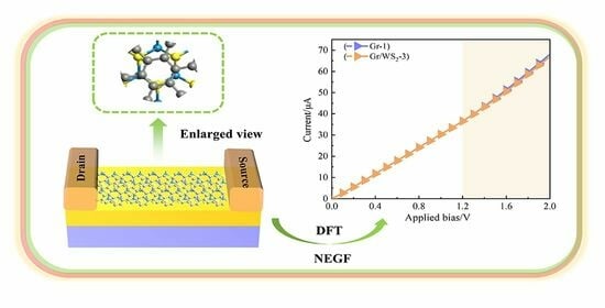
With the Gr/WS
2-3 and Gr-1 (composed of graphene, with the same lattice parameter and rotation angle as Gr/WS
2-3), we built two devices, as depicted in
Figure 4. As seen in the enlarged area, the rotation angle between graphene and WS
2 was still maintained. The poles of the device formed by themselves, the current transport direction was along the Z-axis, and the surface was perpendicular to the X-axis.
The I–V characteristics of the devices in a bias zone [0.0 V, 2.0 V] were calculated to explore the transport characteristics of these two devices, and the findings are shown in
Figure 4. We can see from the current-voltage (I–V) characteristic curves (
Figure 4c) that the heterojunction had comparable transport properties to graphene, unlike some typical heterojunction semiconductor devices. Interestingly, the Ohmic behavior of linear I–V curves was found in the 0–1.2 V bias voltage. After 1.2 V, the slope of the I–V curve gradually increased, leading to nonlinear transport properties. This was caused by a certain degree of rotation in the graphene and heterojunction, while the transport direction was primarily along the armchair direction of the graphene. Simultaneously, it became evident that the transport properties of both devices changed gradually as the voltage increased, signifying a weakened coupling between WS
2 and graphene. A nonlinear relationship only began to emerge at high bias voltages. Compared to other graphene-based heterojunctions, the transport current of graphene/WS
2 was nearly one order of magnitude higher than that of graphene/MoS
2 in-plane heterojunctions [
33,
34], graphene/BN heterojunctions [
35], and so on. In addition, when compared to other WS
2-based heterojunctions, such heterojunctions could behave up to two orders of magnitude higher than that of WS
2/WSe
2 heterojunctions [
36], with greater performance than that of MoS
2/WS
2 heterojunctions [
37]. Thus, we can conclude that such heterojunctions can greatly enhance the transport current and decrease the contact resistance, which will be very important for achieving superior optoelectronic devices such as vertical field-effect transistors (FETs). Our calculations can reveal why graphene/WS
2 heterojunctions are widely used to build FETs and have superior behavioral properties [
38,
39,
40,
41]. In addition, the heterojunction used in our calculations not only maintained the perfect transport properties but also largely reduced the size of the electronic devices, which is very important in the post-Moore era.
Although the differences in transport properties between these two devices were slight, the transport mechanism exhibited different phenomena due to the weak vdW forces between the WS2 and graphene. The most understandable depiction of the behavior of electron transport was the transmission spectrum T(E), and the transmission coefficient of each energy point was determined by diagonalizing the transmission matrix from the eigenvalues of electron transmission. Therefore, we calculated the transmission spectra of the above devices to further study their transport properties.
Generally speaking, the magnitude of the transmission coefficient near the Fermi level represents the transport capability of the device, especially at the Fermi level. The larger the transmission coefficient at the Fermi level, the stronger the transport capability. As shown in
Figure 5a,d, these two devices exhibited metallic properties, corresponding to the current–voltage curves. The electron transmission spectra of graphene devices and Gr/WS
2-3 devices displayed quantum steps between −1 eV and 1 eV, resembling the ideal one-dimensional nanowires. And the electron transmission probability at the Fermi energy level was almost zero, which shows a band gap feature between the conduction and valence bands, corresponding to a Dirac cone in the energy band structure. Although the system had almost no electrons passing through at this energy, at higher energies electrons could easily tunnel through the potential barrier, increasing their mobility and the step transmission coefficient, which indicates that there were several electron transmission channels in these devices. After the formation of the heterojunction, many spikes appeared away from the Fermi energy level, showing that the coupling between the graphene and WS
2 was weak. The band gap of graphene was not open, although it tends to be open, which does not have a significant influence on its transport properties.
To further shed light on the inherent mechanisms of these two devices, we discuss DOS around the Fermi level for these devices.
Figure 5a,d illustrate that the DOS of the two devices were zero at the Fermi energy level, corresponding to their electron transmission spectrum. Before the construction of the heterojunction, the contribution of DOS near the Fermi energy level originated mainly from the 2p orbitals of the graphene carbon atoms. After the formation of the heterojunction, the contribution was mainly from the 2p orbital of the graphene carbon atom and the 5d of the W atom. We can see clearly that several peaks exceeded 100 in the Gr/WS
2-3, more than twice that of the Gr-1. The highest peaks in the valence band region were observed at −1.92 eV, while those in the conduction band region were found at 1.44 eV. These peaks serve to protect fewer delocalized states near the Fermi level.
Here, the dominant transmission eigenstates near the Fermi energy level at equilibrium were calculated to explore the physical roots of their transport phenomena. The calculated results in
Figure 5b,c,e, and f showed that the transmission of two devices around the Fermi level was provided by two major transport channels, both with transmission eigenvalues of nearly 1.000. The transmission eigenstates of both devices exhibited delocalization throughout the whole central region, resulting in significant transport capability near the Fermi energy level. We can see that the electronic states were evenly distributed in the diffusion region between the left and right electrodes, along the graphene armchair direction. This indicates that these states were all π-orbitals of the C atom of graphene, leading to their metallic characteristic. However, the contribution of WS
2 in Gr/WS
2-3 was almost negligible.
It is well known that the study of transmission spectra at non-zero bias voltages can provide useful information for the study of I–V characteristics. This is because the current is defined by the integrated area of the transmission curve within the bias window, as shown by the Landauer–Buttiker formula. As a result, we calculated the transmission spectra of the Gr-1 and Gr/WS
2-3 devices under 0.4, 0.8, 1.2, 1.6, and 2.0 to further reveal their transport phenomena (
Figure 6a,b). The bias window’s perimeter is represented by the colored parts. The effective integral area of the transmission curve within the bias window grew with increased bias, producing a linear I–V characteristic, as we can see from both devices. However, when the bias window increased to 1.2 V, the step transmission spectrum started to change shape and expand in an arc, so the I–V curve began to show non-linear features, and the slope subsequently increased. It is evident from the transmission spectrum that quantum steps are always present within the bias window at different bias voltages and that the steps shift as the bias window expands. The movement tendency of the steps in the conduction and valence band regions was indicated by the arrows, respectively. The number of wave valleys within the bias window in the Gr/WS
2-3 devices progressively increased. Spikes far from the Fermi energy level moved in the opposite direction and were unable to move inside the bias window, so the contribution of these spikes to the transport properties was almost negligible. Interestingly, the lowest transmission probability was always located at the boundary of the bias window, and as the bias increased from 0 V to 2 V, the gap shifted to the boundary of the bias window.
It is worth noting that the transmission eigenstates of electrons may change under external bias after forming the heterojunction. Therefore, the electronic transmission eigenstates of Gr-1 and Gr/WS
2-3 devices were calculated at different bias voltages. Before 2.0 V, the transmission eigenstates of both devices were mainly contributed by the two transmission channels of graphene. However, when the bias voltage increased to 2.0 V, the transmission channels at the Fermi level of Gr/WS
2-3 changed from two to multiple channels, as shown in
Figure 6c,d. WS
2 started to participate in the transport, but its electronic state was localized at the left electrode and the transmission eigenvalue was so small that it can still be disregarded.


