2.1. Theoretical Prediction of Crystallographic and Thermodynamic Stabilities of 0D A3BiCl6
The first-principle calculations were carried out using density functional theory with a plane-wave basis set and projector-augmented wave (PAW) method [
45,
46] as implemented in the Vienna ab initio simulation package (VASP). The geometries and electronic structures were relaxed by the generalized gradient approximation (GGA) in the modified Perdew–Burke–Ernzerhof (PBE) form [
47,
48,
49]. A kinetic-energy cutoff of 350 eV was tested and found to be sufficient for plane-wave expansion to achieve good convergence. The conjugate gradient algorithm was used until the total energy was converged to 10
−5 eV in the electronic self-consistency loop, and a force criterion of 0.01 eV Å was allowed. There were 40 atoms in the A
3BX
6 simulation unit and k points were set as 7 × 7 × 4.
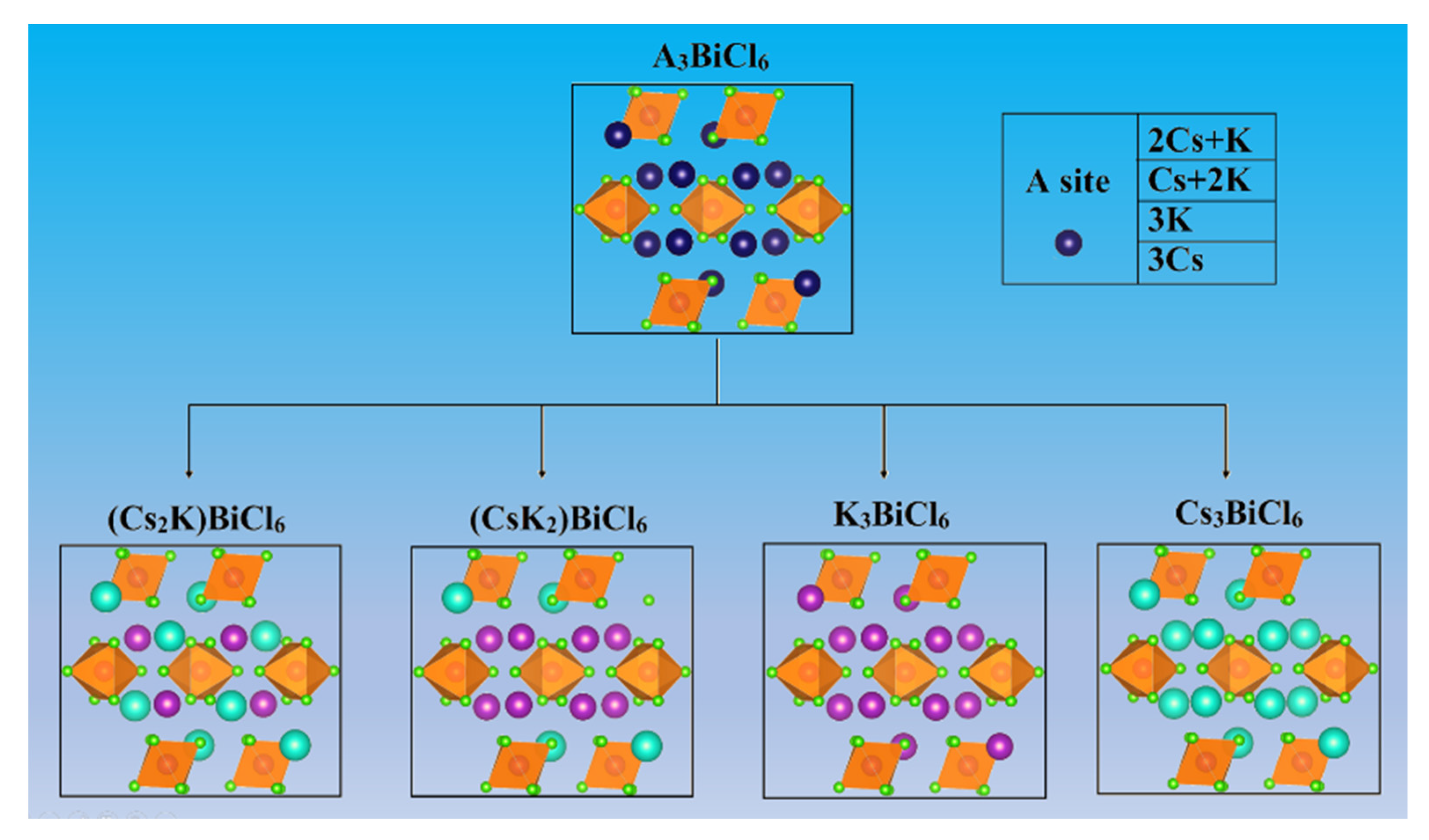
First, we constructed the 0D structures of (Cs
2K)BiCl
6, (CsK
2)BiCl
6, and K
3BiCl
6 through the regulation of the A site (
Figure 1). The 0D (Cs
2K)BiCl
6, (CsK
2)BiCl
6, and K
3BiCl
6 are monoclinic crystal structures with space group C/2c, consistent with 0D Cs
3BiCl
6. In (CsK
2)BiCl
6, the BiCl
63− octahedron is sterically isolated by surrounding Cs
+ and K
+ atoms. The distance between two adjacent Bi atoms in (CsK
2)BiCl
6 is approximately 7.71–7.76 Å, indicating almost no interaction between the two adjacent BiCl
63− octahedra and the nature of 0D electronic dimensionality [
50].
The Goldschmidt empirical criterion was used to evaluate the crystal stability of perovskite structure materials [
51,
52]. Thus, two empirical quantities were obtained: the Goldschmidt tolerance factor (
t) and the octahedral factor (
μ). Previous statistical analysis of all existing halide perovskites has shown that stable perovskite structure formation requires 0.81 <
t < 1.11 and 0.41 <
μ < 0.90. Due to the existence of multiple cations, the formulas for
t and
μ in this paper can be defined as:
where
rCs,
rK,
rBi and
rCl are the Shannon ionic radii of Cs
+, K
+, Bi
3+ and Cl
− ions, respectively. The
t and
μ of the four structures are shown in
Figure 2. Our calculations show that both
t and
μ of Cs
3BiCl
6, (Cs
2K)BiCl
6 and (CsK
2)BiCl
6 are within reasonable ranges, indicating that the Cs
3BiCl
6, (Cs
2K)BiCl
6 and (CsK
2)BiCl
6 compounds are stable perovskite structures. Although K
3BiCl
6 has a
μ = 0.569, within the recommended range, its
t-value of 0.794 suggests that it may form a distorted perovskite structure.
Then, to further evaluate the thermodynamic stabilities of these structures, we calculated their decomposition enthalpies (ΔH
d) with respect to possible decomposition pathways. ΔH
d is defined as the energy difference between the decomposed producers and the A
3BiCl
6 compound. The large positive values of ΔH
d (decomposed into corresponding binary materials) above 20 meV per atom indicate the thermodynamic stability of the A
3BiCl
6 compounds. In the stability assessment, including the possibility of decomposition pathways involving ternary compounds is quite important for quaternary compounds. Therefore, in our calculations, we considered the expected decomposition products reported experimentally, including selected ternary compounds. For (CsK
2)BiCl
6, we have investigated the following possible decomposition pathways:
The reaction pathways for Cs3BiCl6, (Cs2K)BiCl6 and K3BiCl6 are shown in the Supporting Information.
For the four structures, Cs
3BiCl
6, (Cs
2K)BiCl
6 and (CsK
2)BiCl
6 show positive ΔH
d values, while K
3BiCl
6 shows negative ΔH
d values in decomposition paths involving only binary compounds, indicating that K
3BiCl
6 cannot be synthesized stably (
Figure 2). However, when considering ternary compounds, such as Cs
3Bi
2Cl
9, (Cs
2K)BiCl
6 shows negative values, indicating that even if (Cs
2K)BiCl
6 can be synthesized, it would spontaneously decompose into a mixture of Cs
3Bi
2Cl
9 and other binary compounds, so it is difficult to synthesize 0D (Cs
2K)BiCl
6 under thermodynamic equilibrium conditions. This explains why there have been no experimental reports on the successful synthesis of pure 0D (Cs
2K)BiCl
6 so far. For (CsK
2)BiCl
6, the decomposition enthalpy of (CsK
2)BiCl
6 is positive under the decomposition paths of all known compounds, indicating that this structure has good thermodynamic stability and may be synthesized experimentally.
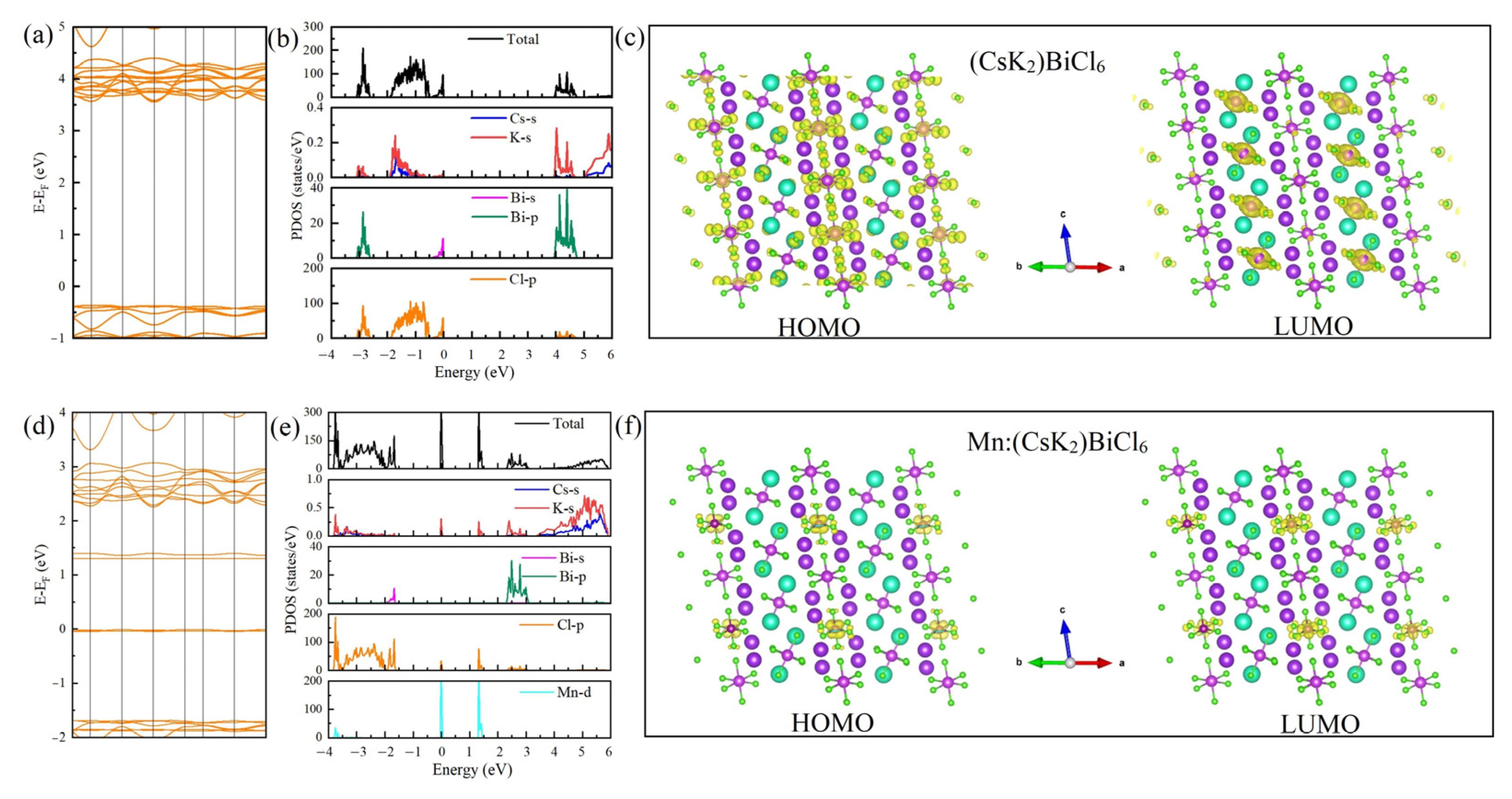
2.2. Electronic Structure of (CsK2)BiCl6
The above studies show that (CsK
2)BiCl
6 is a stable compound, and the electronic properties of (CsK
2)BiCl
6 were investigated using DFT calculations. The energy band structure shows that the indirect bandgap of (CsK
2)BiCl
6 is 3.92 eV (
Figure 3a). Combined with DOS, it can be seen that the valence band maximum (VBM) of (CsK
2)BiCl
6 mainly comes from the s orbital of Bi and the p orbital of Cl, while the conduction band minimum (CBM) is mainly contributed by the p orbital of Bi and Cl (
Figure 3b). In the charge density of
Figure 3c, whether it is HOMO or LUMO, the charge is mainly concentrated between the Bi atom and the Cl atom. This is consistent with our previously calculated results for Cs
3BiCl
6, indicating that the change of the A site has a very negligible effect on the electronic structure of Cs
3BiCl
6. However, it can effectively reduce the proportion of Cs in the compound and expand the compositional space of Bi-based halides.
Similar to Cs
3BiCl
6, the inherent indirect bandgap of (CsK
2)BiCl
6 may lead to its poor PL performance, limiting its further applications. Previous research results show that do** can effectively tune the electronic structure of materials, and experimentally reasonable do** can improve the PL performance of metal halides [
27,
53]. As a suitable metal ion dopant, Mn
2+ has been widely used to tune the optical properties of semiconductors. Therefore, the electronic structure of (CsK
2)BiCl
6 after Mn do** was calculated. We constructed an Mn-doped (CsK
2)BiCl
6 structure by replacing Bi with Mn and optimized it to obtain the most stable crystal structure.
Figure 3d–f shows the energy band structure, DOS and charge density of Mn-doped (CsK
2)BiCl
6, respectively. Compared with pristine (CsK
2)BiCl
6, Mn-do** produces two impurity states in the forbidden band. Combining DOS, it is found that these two impurity states are mainly due to the contribution of the 3D orbital of Mn.
Figure 3f shows the charge density of Mn-doped (CsK
2)BiCl
6. The results show that the charge density around Mn is higher than that of Bi in both HOMO and LUMO. This is mainly due to the different valence states of Mn
2+ and Bi
3+, while the high charge density around Mn explains the charge balance of Mn-doped (CsK
2)BiCl
6.
When light passes through some solid materials, electrons, atoms or ions in the material will interact with the light, resulting in reflection, absorption and projection. The absorption of light by semiconductor materials is mainly divided into intrinsic absorption, lattice vibration absorption and carrier absorption. The absorption spectrum is calculated from the dielectric function equation [
54]:
where
ε1 and
ε2 correspond to the real and imaginary parts of the dielectric function, respectively. Usually, the interaction between the dopant atoms and the substrate leads to enhanced optical properties of the doped structure.
Figure S1 (see in Supplementary Materials) calculates the optical absorption of undoped and Mn-doped (CsK
2)BiCl
6. Compared with pristine (CsK
2)BiCl
6, the absorption coefficient of Mn-doped (CsK
2)BiCl
6 moves in the lower energy direction, the absorption edge is red-shifted, and the energy corresponding to the peak of the absorption coefficient is consistent with the dielectric function (
Figure S2). In the 1.2–4.4 eV region, the absorption coefficient of Mn-doped (CsK
2)BiCl
6 was significantly enhanced, indicating that Mn-doped (CsK
2)BiCl
6 has a better absorption effect on visible light.
2.3. Experimental Crystal Structure of (CsK2)BiCl6
The pristine 0D (CsK
2)BiCl
6 crystals were synthesized with a simple solvothermal method. The detailed experimental method is described in the supporting information.
Figure S3 shows the powder X-ray diffraction (PXRD) pattern of the samples. The theoretical XRD results match well with simulated XRD patterns and show no impurity formation.
To understand the optical properties of 0D (CsK
2)BiCl
6, the absorption and PL spectra of the material were tested. The PL spectrum has no emission at room temperature, which may be due to the indirect bandgap properties of the material. The recombination process of the excited state band edge in the indirect bandgap material needs the assistance of phonons, making the nonradiative recombination dominant, thus, reducing the radiative recombination process, and in turn resulting in its poor PL performance [
55].
Figure S4 shows the absorption spectrum and Tauc plot diagram of (CsK
2)BiCl
6. The absorption spectrum shows that 0D (CsK
2)BiCl
6 has absorption characteristics between 250 and 400 nm, especially at 260, 320 and 360 nm. These characteristic absorption peaks come from the 6s2 to 6s1p1 transition in the BiCl
63− octahedron. The Tauc plot shows that the material has two linear band edge intercepts of 3.29 and 4.02 eV, respectively, which is similar to that of Cs
2NaBiCl
6 [
56]. The experimental bandgap value of the (CsK
2)BiCl
6 material is 4.02 eV, which is higher than the theoretical calculation result (3.8 eV). This computed bandgap is lower than the experimentally estimated bandgap because standard DFT calculations usually underestimate the bandgap of the material.
Mn
2+ ion is widely used for improving and regulating the optical properties and band structure of materials [
57,
58,
59]. For the poor optical properties of (CsK
2)BiCl
6, Mn
2+ do** is expected to enhance its luminescence and make it a candidate material for optoelectronic device applications. A series of (CsK
2)BiCl
6 metal halides doped with different Mn
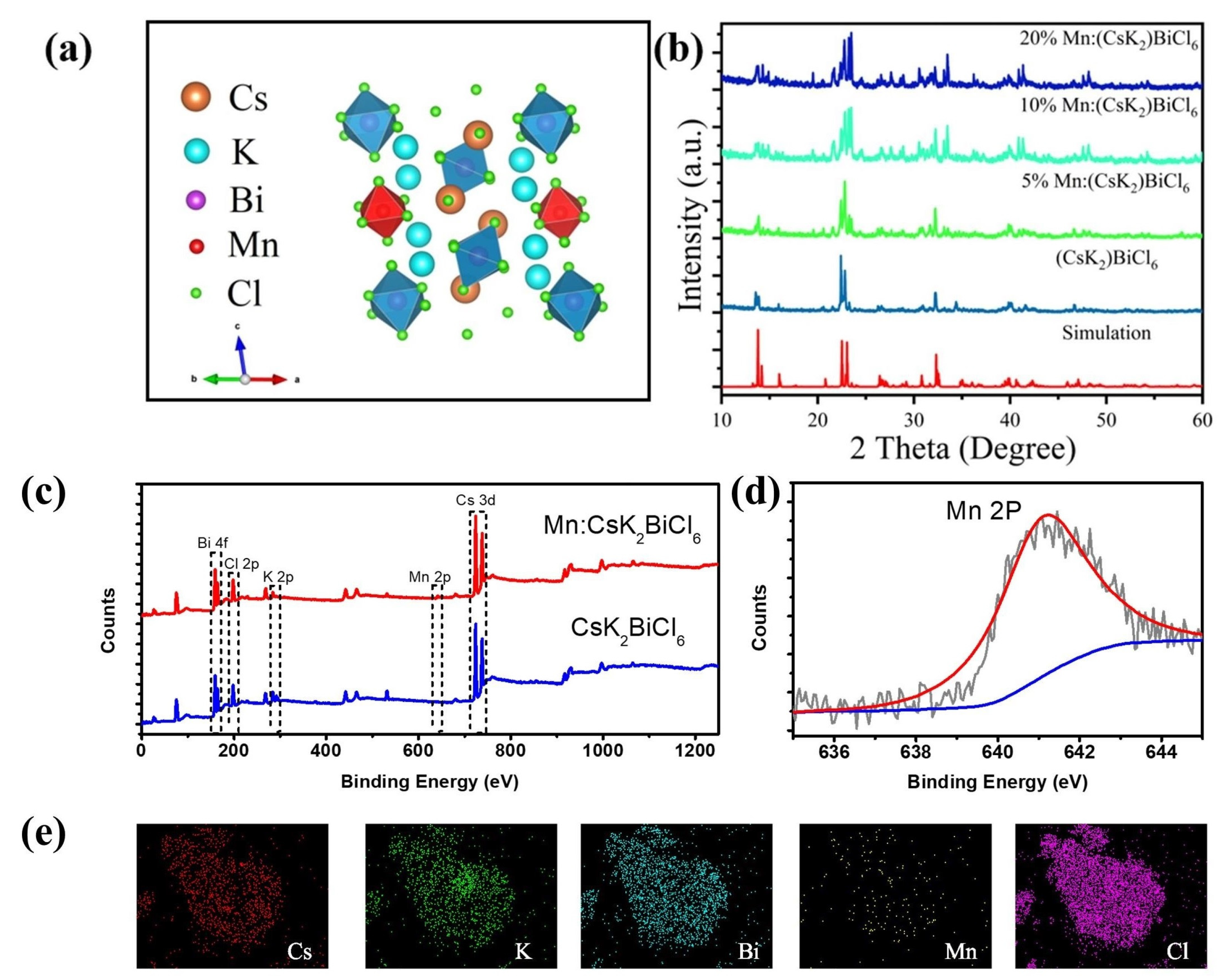
2+ concentrations were synthesized. The schematic structure of Mn-doped (CsK
2)BiCl
6 is shown in
Figure 4a. Mn
2+ ions are doped into the lattice to replace Bi
3+ to form an isolated MnCl
64- structure. The PXRD patterns of (CsK
2)BiCl
6 doped with different Mn
2+ concentrations are shown in
Figure 4b. The do** of Mn
2+ ions do not show any new impurity peaks. The overall peak position is consistent with the pristine (CsK
2)BiCl
6. The results show that Mn
2+ do** does not destroy the structure of the host (CsK
2)BiCl
6.
The X-ray photoelectron spectra (XPS) further confirmed that Mn
2+ ions were successfully doped into (CsK
2)BiCl
6 and Mn
2+ do** does not produce extra phase (
Figure 4c).
Figure 4d shows the high-resolution XPS spectra and peak fitting of Mn 2p. The peak at 641.0 eV is attributed to Mn 2p.
Figure S5 shows the high-resolution XPS spectra of Cs, K, Bi and Cl in the samples. Compared with the pristine sample, the binding energies of Cs, K and Bi in the Mn-doped sample are slightly increased, which shows that the electron distribution of the Mn-doped samples is more compact. The composition and distribution of elements in a sample are usually determined using scanning electron microscope (SEM) images and an energy disperse spectrometer (EDS),
Figures S6a and 4e are the SEM image and EDS spectra of 10%Mn: (CsK
2)BiCl
6, respectively. The results show that Cs, K, Bi, Cl and Mn elements are uniformly distributed in the lattice.
Figure S6b shows the element content measured in selected local areas of 10%Mn: (CsK
2)BiCl
6 sample. The basic atomic ratio of (Cs + K):Bi:Cl is approximately 3:1:6. By using 9:1 of the nominal Bi/Mn ratio, but the actual measured Mn content is 7.5%.
2.4. Optical Properties of (CsK2)BiCl6
Previous studies have shown that the efficient luminescence center and energy transfer acceptor of Mn
2+ ions can effectively improve the optical properties of materials. Therefore, the optical properties of the 10%Mn:(CsK
2)BiCl
6 sample were investigated.
Figure 5a shows the absorption spectra of 10%Mn:(CsK
2)BiCl
6 and pristine (CsK
2)BiCl
6 samples, respectively. For the pristine (CsK
2)BiCl
6, the BiCl
63− octahedrons have a strong absorption at 260, 320 and 360 nm due to the 6s
2→6s
1p
1 transition in Bi
3+. The 10%Mn:(CsK
2)BiCl
6 sample has the similar absorption characteristics as the pristine (CsK
2)BiCl
6 sample before 380 nm, the overall absorption peak position and shape are consistent. The main reason is that the absorption peak in this interval comes from the characteristic absorption of BiCl
63− octahedrons. However, the 10%Mn:(CsK
2)BiCl
6 sample has an additional absorption peak at 430 and 520 nm, which is from the
6A
1g to
4T
1g absorption transition of Mn
2+.
Figure 5b shows the PLE and PL spectra of 10%Mn:(CsK
2)BiCl
6 sample. The excitation spectra show three main excitation peaks that correspond to the absorption spectra. The excitation peaks less than 400 nm come from the transition from the ground state
1S
0 of Bi
3+ to the excited states
3P
1 and
1P
1. The excitation peaks larger than 400 nm come from Mn
2+ characteristic transitions. The PL spectra show that, compared with pristine (CsK
2)BiCl
6, the material achieves bright orange emission at 605 nm through Mn
2+ do** modification. Under the excitation of different wavelengths, such as 295, 365 and 430 nm, the peak position and peak shape of the PL spectrum are consistent. In addition, the peak shapes and positions of the excitation spectra measured with different emission wavelengths remain consistent, and the results are shown in
Figure S7. The PL intensity is highest under the optimal excitation wavelength (365 nm), which suggests that the observed emission is actually from the intrinsic states of the samples, rather than nonradiative transitions, such as lattice defects and surface states.
The photophysical mechanism of 10%Mn:(CsK
2)BiCl
6 is shown in
Figure 5c. Under the excitation of UV light, the electron absorbs energy and transitions from the valence band to the conduction band. For undoped samples, due to the nature of the indirect bandgap, most of the energy is lost through phonon vibration. The carriers in the conduction band cannot be transferred to self-trapped excitons or formed into self-trapped excitons, resulting in very poor luminescent performance. For Mn-doped samples, combined with the previous theoretical calculation, Mn do** can form an impurity state in the energy band structure, and the excited state carriers can effectively relax to the
4T
1 state of Mn
2+, and transition from the
4T
1 state to the
6A
1 state, during this process, photons are emitted, and a bright orange light emission is produced.
Figure S8 shows the PL spectra of pristine (CsK
2)BiCl
6 and x%Mn:(CsK
2)BiCl
6, and the pristine sample exhibits very poor optical properties. After Mn
2+ do**, the sample exhibits a broadband emission at 605 nm, and the emission peak intensity gradually increases with increasing Mn-do** concentration. When the Mn
2+ do** concentration is 10%, the PL intensity of the system reaches its highest.
Figure 5d shows the time-resolved PL lifetimes of 5%, 10% and 20% of Mn
2+ doped (CsK
2)BiCl
6 samples monitored at 605 nm. The curve can be fitted by a double exponential function A(t) = A
1exp(−t/τ
1) + A
2exp(−t/τ
2), where A(t) is the time change in PL intensity at time t, τ
1/τ
2 represents the lifetime of different recombination processes, and A
1/A
2 is the corresponding weight. The fitting data are shown in
Table S1. The results show that the samples in the system exhibit a submillisecond lifetime, which is consistent with the typical characteristics of the PL lifetime of Mn
2+ ions.
The intrinsic photophysical properties of (CsK
2)BiCl
6 are further revealed, and the temperature-dependent emission spectra of Mn-doped systems are measured.
Figure 5e shows the PL spectrum of 10%Mn:(CsK
2)BiCl
6 in the temperature range of 80~360 K. Similar to common metal halides, the PL intensity increases significantly at low temperatures, which is due to the weakening of electron-phonon coupling with decreasing temperature, thereby suppressing nonradiative recombination. The PL intensity decreases as the temperature increases from 80 to 360 K, which is consistent with the model that more and more phonons participate in intensifying nonradiative recombination at high temperatures. It is worth noting that the PL peak position of the sample shifted slightly with temperature. As shown in
Figure S9, with the temperature increasing from 80 to 360 K, the central peak position shifted from 630 to 605 nm. This is because the increase in temperature leads to the expansion of the lattice, thereby increasing the Mn-Mn spacing. The luminescence of Mn
2+ is closely related to the Mn-Mn spacing. The increase in spacing makes the interaction between Mn-Mn weaken, resulting in an increase in the energy level difference of
4T
1—
6A
1.
Figure 5f shows a pseudo color plot of temperature-dependent PL intensity and wavelength. Compared with the PL intensity at low temperature, the luminescence quenching occurred at 300 K, indicating that the luminescence performance of the material at room temperature is poor.
Figure S10 shows the full width at half maximum (FWHM) as a function of temperature, and the results show that FWHM increases significantly with increasing temperature. The electron-phonon coupling in a soft halide matrix leads to a larger FWHM with increasing temperature. However, excessive electron-phonon coupling can cause energy to be dissipated by vibrations of phonons, leading to the predominance of nonradiative recombination and degrading the luminescent properties of the material. In general, improving the optical properties of bismuth-based perovskite materials requires solving the strong electron-phonon coupling characteristics inside the material and enhancing its exciton binding energy. How to effectively improve these two factors is the solution and strategy to solve the poor optical properties of such materials, and the design and regulation of future materials should be broken through and improved in this direction.


