
Progress in Ammonothermal Crystal Growth of Gallium Nitride from 2017–2023: Process, Defects and Devices

Abstract
:1. Introduction
2. Growth Methods and Technology
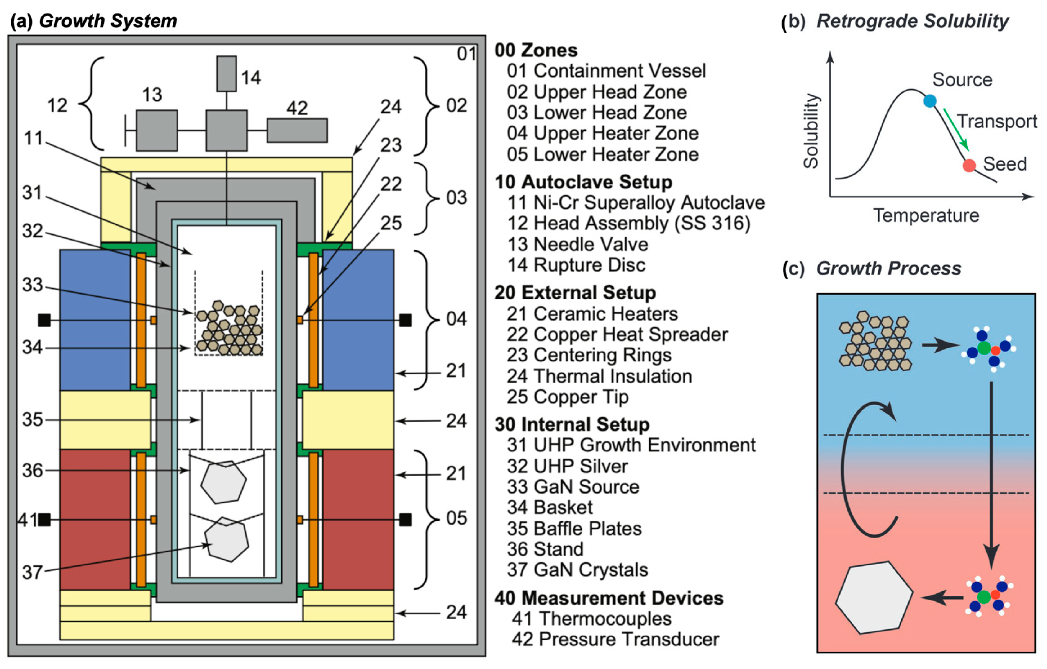
2.1. Progress in Growth Methods
2.2. In Situ Measurements of Ammonothermal Growth
3. Characterization Methods and GaN Material Properties
3.1. Structural Defects
3.2. Do**
3.3. Point Defects and Impurities
4. Device Performance Results
5. Conclusions
Author Contributions
Funding
Data Availability Statement
Conflicts of Interest
References
- Maruska, H.P.; Tietjen, J.J. The Preparation and Properties of Vapor-Deposited Single-Crystal GaN. Appl. Phys. Lett. 1969, 15, 327. [Google Scholar] [CrossRef]
- Nakamura, S.; Fasol, G. The Blue Laser Diode—GaN-Based Light Emitters and Lasers; Springer: Berlin, Germany, 1997; ISBN 987-3-662-03464-4S. [Google Scholar]
- Yoshida, T.; Oshima, Y.; Watanabe, K.; Tsuchiya, T.; Mishima, T. Ultrahigh-speed growth of GaN by hydride vapor phase epitaxy. Phys. Status Solidi 2011, 8, 2110–2112. [Google Scholar] [CrossRef]
- Kucharski, R.; Sochacki, T.; Lucznik, B.; Amilusik, M.; Grabianska, K.; Iwinska, M.; Bockowski, M. Ammonothermal and HVPE Bulk Growth of GaN. In Wide Bandgap Semiconductors for Power Electronics: Materials, Devices, Applications; Wellmann, P., Ohtani, N., Rupp, R., Eds.; Wiley-VCH GmbH: Weinheim, Germany, 2021; Chapter 18. [Google Scholar] [CrossRef]
- Baliga, B.J. Gallium nitride devices for power electronic applications. Semicond. Sci. Technol. 2013, 28, 074011. [Google Scholar] [CrossRef]
- Marino, F.A.; Faralli, N.; Ferry, D.K.; Goodnick, S.M.; Saraniti, M. Figures of merit in high-frequency and high-power GaN HEMTs. J. Phys. Conf. Ser. 2009, 193, 012040. [Google Scholar] [CrossRef]
- Hickman, A.L.; Chaudhuri, R.; Bader, S.J.; Nomoto, K.; Li, L.; Hwang, J.C.; ** of GaN substrates and epitaxial layers used for power electronic devices by synchrotron X-ray rocking curve topography. J. Cryst. Growth 2022, 583, 126559. [Google Scholar] [CrossRef]
- Kirste, L.; Grabianska, K.; Kucharski, R.; Sochacki, T.; Lucznik, B.; Bockowski, M. Structural Analysis of Low Defect Ammonothermally Grown GaN Wafers by Borrmann Effect X-ray Topography. Materials 2021, 14, 5472. [Google Scholar] [CrossRef] [PubMed]
- Stoddard, N. Methods and Apparatus for Manufacturing Monocrystalline Cast Silicon and Monocrystalline Cast Silicon Bodies for Photovoltaics. U.S. Patent 8628614B2, 14 January 2014. [Google Scholar]
- Stoddard, N. Seed Layers and Process of Manufacturing Seed Layers. U.S. Patent 8882077B2, 11 November 2014. [Google Scholar]
- Kutsukake, K.; Usami, N.; Ohno, Y.; Tokumoto, Y.; Yonenaga, I. Mono-Like Silicon Growth Using Functional Grain Boundaries to Limit Area of Multicrystalline Grains. IEEE J. Photovolt. 2014, 4, 84–87. [Google Scholar] [CrossRef]
- Trempa, M.; Reimann, C.; Friedrich, J.; Muller, G.; Krause, A.; Sylla, L.; Richter, T. Influence of grain boundaries intentionally induced between seed plates on the defect generation in quasi-mono-crystalline silicon ingots. Cryst. Res. Technol. 2014, 50, 124–132. [Google Scholar] [CrossRef]
- Zhang, F.; Yu, X.; Liu, C.; Yuan, S.; Zhu, X.; Zhang, Z.; Huang, L.; Lei, Q.; Hu, D.; Yang, D. Designing functional Σ13 grain boundaries at seed junctions for high-quality cast quasi-single crystalline silicon. Sol. Energy Mater. Sol. Cells 2019, 200, 109985. [Google Scholar] [CrossRef]
- Schubert, M.; Schindler, F.; Benick, J.; Riepe, S.; Krenckel, P.; Richter, A.; Muller, R.; Hammann, B.; Nold, S. The potential of cast silicon. Sol. Energy Mater. Sol. Cells 2021, 219, 110789. [Google Scholar] [CrossRef]
- Hashimoto, T.; Letts, E.R.; Key, D.; Jordan, B. Two inch GaN substrates fabricated by the near equilibrium ammonothermal (NEAT) method. Jpn J. Appl. Phys. 2019, 58, SC1005. [Google Scholar] [CrossRef]
- Hashimoto, T.; Letts, E.R.; Key, D.; Jordan, B.; Shang, E. GaN Substrate development through the near equilibrium ammonothermal (NEAT) method and its application to higher performance GaN-based devices. In Proceedings of the SPIE Quantum Sensing and Nano Electronics and Photonics XVI, San Francisco, CA, USA, 3–7 February 2019; p. 10926. [Google Scholar]
- Tomida, D.; Bao, Q.; Saito, M.; Kurimoto, K.; Sato, F.; Ishiguro, T.; Chichibu, S.F. Effects of extra metals added in an autoclave during acidic ammonothermal growth of m-plane GaN single crystals using an NH4F mineralizer. Appl. Phys. Express 2018, 11, 091002. [Google Scholar] [CrossRef] [Green Version]
- Heikkinen, T.; Pavlov, J.; Ceponis, T.; Gaubas, E.; Zajac, M.; Tuomisto, F. Effect of Mn and Mg dopants on vacancy defect formation in ammonothermal GaN. J. Cryst. Growth 2020, 547, 125803. [Google Scholar] [CrossRef]
- Zajac, M.; Konczewicz, L.; Litwin-Staszewska, E.; Iwinska, M.; Kucharski, R.; Juillaguet, S.; Contreras, S. P-type conductivity in GaN:Zn monocrystals grown by ammonothermal method. J. Appl. Phys. 2021, 129, 135702. [Google Scholar] [CrossRef]
- Amilusik, M.; Sohacki, T.; Fijalkowski, M.; Lucznik, B.; Iwinska, M.; Sidor, A.; Teisseyre, H.; Domagala, J.; Grzegory, I.; Bockowski, M. Homoepitaxial growth by halide vapor phase epitaxy of semi-polar GaN on ammonothermal seeds. Jpn J. Appl. Phys. 2019, 58, SC1030. [Google Scholar] [CrossRef]
- Reschikov, M.A.; Demchenko, D.O.; Ye, D.; Andrieiev, O.; Vorobiov, M.; Grabianska, K.; Zajac, M.; Nita, P.; Iwinska, M.; Bockowski, M.; et al. The effect of annealing on photoluminescence from defects in ammonothermal GaN. J. Appl. Phys. 2022, 131, 035704. [Google Scholar] [CrossRef]
- Jiang, W.; Nolan, M.; Ehrentraut, D.; D’Evelyn, M.P. Electrical and optical properties of gallium vacancy complexes in ammonothermal GaN. Appl. Phys. Express 2017, 10, 075506. [Google Scholar] [CrossRef]
- Suihkonen, S.; Pimputkar, S.; Speck, J.S.; Nakamura, S. Infrared absorption of hydrogen-related defects in ammonothermal GaN. Appl. Phys. Lett. 2016, 108, 202105. [Google Scholar] [CrossRef] [Green Version]
- Tuomisto, F.; Kuittinen, T.; Zając, M.; Doradziński, R.M.; Wasik, D. Vacancy–hydrogen complexes in ammonothermal GaN. J. Cryst. Growth 2014, 403, 114–118. [Google Scholar] [CrossRef]
- Polyakov, A.Y.; Smirnov, N.B.; Shchemerov, I.V.; Gogova, D.; Tarelkin, S.A.; Lee, I.; Pearton, S.J. Electrical Properties of Bulk, Non-Polar, Semi-Insulating M-GaN Grown by the Ammonothermal Method. ECS J. Solid State Sci. Technol. 2018, 7, P260. [Google Scholar] [CrossRef]
- Chen, S.-W.H.; Wang, H.; Hu, C.; Chen, Y.; Wang, H. Vertical GaN-on-GaN PIN diodes fabricated on free-standing GaN wafer using an ammonothermal method. J. Alloy Compd. 2019, 804, 435–440. [Google Scholar] [CrossRef]
- Key, D.; Letts, E.; Tsou, C.; Ji, M.; Bakhtiary-Noodeh, M.; Detchprohm, T.; Shen, S.; Dupuis, R.; Hashimoto, T. Structural and Electrical Characterization of 2″ Ammonothermal Free-Standing GaN Wafers. Progress toward Pilot Production. Materials 2019, 12, 1925. [Google Scholar] [CrossRef] [Green Version]
- Taube, A.; Kaminski, M.; Tarenko, J.; Sadowski, O.; Ekielski, M.; Szerling, A.; Prystawko, P.; Bockowski, M.; Grzegory, I. High Breakdown Voltage and High Current Injection Vertical GaN-on-GaN p-n Diodes with Extremely Low On-Resistance Fabricated on Ammonothermally Grown Bulk GaN Substrates. IEEE Trans. Electron Devices 2022, 69, 6255–6259. [Google Scholar] [CrossRef]
- Talesara, V.; Zhang, Y.; Vangipuram, V.G.T.; Zhao, H.; Lu, W. Vertical GaN-on-GaN pn power diodes with Baliga figure of merit of 27 GW/cm2. Appl. Phys. Lett. 2023, 122, 123501. [Google Scholar] [CrossRef]


| Units | IIHP/NL3 | SixPoint | Tohoku/MCC | Soraa/Kyocera | Competition | |
|---|---|---|---|---|---|---|
| Method | Am-GaN-B | NEAT | SCAAT/LPAAT | SCoRA | HVPE | |
| Chemistry | Basic | Basic | Acidic | Acidic | GaCl3-NH3 | |
| Wafer Size | cm | 50–60 | 50–100 | 50–60 | 50 (2015) | 50–150 |
| Growth Rate | mm/day | 24–60 | 30 | 170–205 | 700 | 2400 |
| Temp. Range | deg. C | 400–750 | 450–600 | 550–625 | 650–800 | 900–1100 |
| Press. Range | MPa | 100–600 | 100–300 | 100–200 | 100–600 | Low |
| Oxygen | atoms/cm3 | 1018–2 × 10¹⁹ | 2–8 × 10¹⁸ | - | 1018 | 1017–1019 |
| DD | defects/cm2 | 103–5 × 10⁴ | 105 | 1–5 × 10⁴ | 105 | 5 × 10⁶–108 |
| Curvature | m | >20 | 20 | 1460 | >20 | 1–5 |
| Rocking Width | arcsec | <30 | 20–50 | 20–30 | <30 | 30–80 |
| Boule Thickness | mm | 3–4 | 1–3 | 2–3 | >2 | 3–4 |
| Crystals/run | # | 36 | 50 | - | - | 1 |
| Dislocation Method | Units | Confocal Raman | Synchrotron XRT | Defect Etching | CL | PL | Bevel Etching | Borrmann XRT | HR-XRD |
|---|---|---|---|---|---|---|---|---|---|
| Sample Area | mm2 | 0.0025 | 2500 | 0.25 | 2500 | 2500 | 0.25 | 2500 | 4 |
| Dislocation Ty**? | Yes | Yes | No | No | No | Yes | Yes | No | |
| Destructive? | No | No | Yes | No | No | Yes | No | No | |
| In-line Potential? | No | No | No | Maybe | Yes | No | Yes | Yes | |
| Range Capability | Disl/cm2 | <106 | 102–106 | 102–5 × 10⁶ | - | - | - | <105 | >104 |
| Measurement Depth | Surface | Full Depth | Surface | Surface | Full Depth | Full Depth | Full Depth | Full Depth | |
| 3D Depth Contrast | mm | 2–25 | N/A | N/A | N/A | N/A | 5–400 | N/A | N/A |
| Element | Typical Range (atoms/cm3) | Amilusik Range (atoms/cm3) | Change |
|---|---|---|---|
| H | 1 × 10¹⁹ to 6 × 10²⁰ | 4 × 10¹⁸ to 5 × 10¹⁹ | Improvement |
| C | High 1016 to Low 1017 | 8 × 10¹⁶ to 1.5 × 10¹⁸ | Similar to worse |
| Si | Low 1018 | 1 × 10¹⁷ to 2 × 10¹⁸ | Similar |
| Na | 1 × 10¹⁶ to 1 × 10¹⁹ | 1 × 10¹⁶ to 7 × 10¹⁷ | Similar to better |
| Mg | High 1016 to Low 1017 | 5 × 10¹⁵ to 8 × 10¹⁷ (dopant) | Similar |
| Mn | 3 × 10¹⁶ to 2 × 10¹⁸ | 6 × 10¹⁵ to 1 × 10¹⁸ (dopant) | Similar |
| Fe | ~1016 to Low 1017 | 3 × 10¹⁵ to 2 × 10¹⁶ | Improvement |
| Zn | Not reported | 8 × 10¹⁶ to 2.5 × 10¹⁸ | N/A |
Disclaimer/Publisher’s Note: The statements, opinions and data contained in all publications are solely those of the individual author(s) and contributor(s) and not of MDPI and/or the editor(s). MDPI and/or the editor(s) disclaim responsibility for any injury to people or property resulting from any ideas, methods, instructions or products referred to in the content. |
© 2023 by the authors. Licensee MDPI, Basel, Switzerland. This article is an open access article distributed under the terms and conditions of the Creative Commons Attribution (CC BY) license (https://creativecommons.org/licenses/by/4.0/).
Share and Cite
Stoddard, N.; Pimputkar, S. Progress in Ammonothermal Crystal Growth of Gallium Nitride from 2017–2023: Process, Defects and Devices. Crystals 2023, 13, 1004. https://doi.org/10.3390/cryst13071004
Stoddard N, Pimputkar S. Progress in Ammonothermal Crystal Growth of Gallium Nitride from 2017–2023: Process, Defects and Devices. Crystals. 2023; 13(7):1004. https://doi.org/10.3390/cryst13071004
Chicago/Turabian StyleStoddard, Nathan, and Siddha Pimputkar. 2023. "Progress in Ammonothermal Crystal Growth of Gallium Nitride from 2017–2023: Process, Defects and Devices" Crystals 13, no. 7: 1004. https://doi.org/10.3390/cryst13071004