1. Introduction
Antimony (Sb)-based high-electron, high–hole mobility III–V binary (InSb, GaSb, AlSb), ternary (InAlSb, InGaSb, GaAlSb), and quaternary (InGaAlSb, InGaPSb, InAlPSb, GaAlPSb, InGaPSb) alloys and heterostructures (quantum wells (QWs) including superlattices (SLs)) have attracted a great deal of attention due to their promises for develo** next-generation high-speed infrared opto-electronic and thermo-electric devices [
1,
2,
3,
4,
5,
6,
7,
8,
9,
10,
11,
12,
13,
14,
15]. Among others, the indium-based pnictides (InX; X = P, As, and Sb) have recently gained considerable importance. Although the lowest bandgap
(≡0.18 eV) of InSb material is critical for mid-infrared optoelectronics, ultrathin films, QWs, and SLs involving InP (
≡ 1.35 eV) and InAs (
≡ 0.35 eV) are being used to design metal oxide–semiconductor field-effect transistors (MOSFETs), bipolar junction transistors (BJTs), multi-junction solar cells, light-emitting/receiving devices, infrared detectors (IDs), Shockley diodes (SDs), long-wavelength laser diodes (LDs), photodetectors (PDs), thermoelectric generators (TEGs), etc. [
1,
2,
3,
4,
5,
6,
7,
8,
9,
10,
11,
12,
13,
14,
15,
16]. According to Talazac et al. [
17], several Schottky devices have been integrated recently into different ecosystems for detecting radiation, harmful gases, and pollutants (e.g., ozone O
3, nitrogen oxide NO
3, etc.) and monitoring chemical exposure in the environment. Other devices are also used in satellite communication equipment, high-speed/low-power circuits for bio-medical diagnostics, drug analysis, etc.
As compared to the conventional III–V semiconductors, the growth of InP(As)Sb and/or In(Ga,Al)PSb materials has been and still is quite difficult [
18]. As active cladding layers, the exploitation of ultrathin InP
1−xSb
x alloy films is considered indispensable for mid-infrared (MIR) laser sources. Due to a large ~10.4% lattice mismatch between InP and InSb, the growth of defect-free crystalline thin films of InP
1−xSb
x ternary alloys is quite challenging. Other issues of preparing Sb-based device structures are linked to the (i) low vapor pressure of Sb, (ii) limitations of the kinetically controlled growth regime, (iii) inexistence of chemically stable hydrides as precursors, and (iv) lack of insulating substrates [
16,
17,
18,
19,
20,
21,
22,
23,
24,
25,
26,
27,
28,
29,
30,
31,
32,
33,
34,
35,
36,
37,
38]. Despite these difficulties, several attempts have been made to prepare Sb-based alloys, QWs, and SLs by using liquid-phase epitaxy (LPE), organo-metallic vapor-phase epitaxy (OMVPE), and molecular beam epitaxy (MBE) techniques [
39,
40,
41]. There are still a few intrinsic issues that inhibit the design of several important device structures. However, solutions to these problems can be achieved by exploiting appropriate experimental [
1,
2,
3,
4,
5,
6,
7,
8,
9,
10,
11,
12,
13,
14,
15,
16,
17] and/or theoretical techniques [
18].
Despite many efforts made to grow diverse Sb-based structures, there are limited studies assessing their optical and vibrational characteristics. The experimental methods used for material characterizations include high-resolution X-ray diffraction (HR-XRD) [
39,
40], Fourier transform infrared (FTIR) [
42,
43,
44], Raman scattering spectroscopy (RSS) [
45,
46], photoluminescence (PL) [
25,
26,
27,
47], inelastic neutron scattering (INS) [
48,
49], inelastic X-ray scattering (IXS) [
50], reflection high-energy electron diffraction (RHEED), transmission electron microscopy (TEM) [
35,
36,
37,
38], spectroscopic ellipsometry (SE) [
28,
29], etc. While HR-XRD [
39,
40], FTIR [
42,
43,
44], and RSS have played [
45,
46] vital roles in appraising the alloy composition x, film thickness d, interfacial structure, and surface relaxation of atoms, their exploitation to assess basic properties of Sb-based ternary and quaternary alloys remained, however, surprisingly enigmatic.
For InP
1−xSb
x alloys, there exist few experimental and theoretical studies, especially on the physics of those attributes which ascertain their prominence at a practical level [
1,
2,
3,
4,
5,
6,
7,
8,
9,
10,
11,
12,
13,
14,
15,
16,
17]. In the far-infrared (FIR) region, 5 meV ≤ E ≤ 100 meV, although SE is recognized as an efficient method for exploring lattice dynamics and free carrier concentration of binary materials, the method has not yet been applied to ternary alloys. Earlier analysis of RSS data on vibrational properties of InP
1−xSb
x using a modified random-element iso-displacement (MREI) model envisioned a two-phonon-mode behavior [
25,
26,
27]. However, no gap (In
P:Sb for x
→ 0) or localized vibrational mode (LVM) (In
Sb:P for x
→ 1) was detected near the limiting values of x. Extensive PL measurements and extended X-ray absorption fine-structure (EXAFS) results on Gas-Source Molecular Beam Epitaxy (GS-MBE)-grown InP
1−xSb
x/n-InAs samples have recently provided valuable electronic and structural characteristics [
51]. On the contrary, no attempts have been made to comprehend the optical properties of InP
1−xSb
x alloys in the near-IR (NIR) to ultraviolet (UV) energy range.
The purpose of this paper is to report the results of both experimental (
Section 2) and theoretical (
Section 3) studies to assess the phonon and optical traits of nearly ~1 μm thick InP
1−xSb
x/n-InAs samples grown by the GS-MBE technique (
Section 2.1). The TEM method was employed earlier for investigating the structural and chemical distributions of atoms. The composition of Sb in InP
1−xSb
x alloys has also been achieved by using electron probe microanalysis (EPMA). Room-temperature (RT) Hall measurements with van der Pauw methods have been performed to assess the electrical properties of Be- and Si-doped InP
1−xSb
x epilayers [
39,
40]. Here, we employed a Reinshaw InVia Raman (
Section 2.2) spectrometer with a diode-pumped solid-state (DPSS) 532 nm laser as an excitation source for measuring the composition-dependent longitudinal optical (
) and transverse optical (
) phonons in InP
1−xSb
x/n-InAs samples. The PL measurements are also reported by calibrating the radiation lines of a Xe lamp and employing the SPEX 500M monochromator (
Section 2.3). Like HR-XRD, the PL studies on InP
1−xSb
x/n-InAs samples with smaller values of x (≡0.10, 0.16, 0.17) have confirmed the two energy phases, and for x ≥ 0.30, it provided a single energy phase. From a theoretical standpoint (
Section 3.1), a classical “Drude-Lorentz”model is adopted by incorporating optical
phonons to simulate (
Section 3.2) the complex dielectric functions [
(5 meV ≤ E ≤ 100 meV) energy region for both binary and ternary alloys. Although the optical measurements by SE in the NIR
UV (0. 5 eV to 6.0 eV) energy regions are known for InP and InSb materials [
22,
23], little to no information is available for the ternary InP
1−xSb
x alloys. From technical and scientific perspectives, it is crucial to derive analytical expressions for simulating the optical constants of both binary and ternary alloys. The systematic assessment of refractive indices
and absorption coefficients
is especially important for selecting apposite materials in structural designs and the optimization of different optoelectronic devices. By adopting Adachi’s [
37,
38] optical dispersion mechanisms and using a modified dielectric function (MDF) approach (
Section 3.3 and
Section 3.3.1,
Section 3.3.2 and
Section 3.3.3), we have systematically analyzed the complex dielectric functions of direct bandgap binary InP, InSb materials in the NIR
UV region. This methodology is meticulously extended to obtain the optical constants of InP
1−xSb
x ternary alloys for any arbitrary composition x and photon energy E [≡
. For InP
0.67Sb
0.33 alloy, our MDF simulation has provided the lowest bandgap energy
(near ~0.46 eV), in reasonably good agreement with the existing first-principles calculations [
18] and PL measurements. Theoretical results of phonons and optical traits are compared/contrasted and discussed against the existing experimental data (
Section 4.1,
Section 4.1.1,
Section 4.1.2,
Section 4.2,
Section 4.2.1 and
Section 4.2.2), with concluding remarks presented in
Section 5. We strongly feel that our RSS and PL studies have provided valuable information on the phonon and optical traits of InP
1−xSb
x/n-InAs (001) epilayers and can be extended to many other technologically important materials.
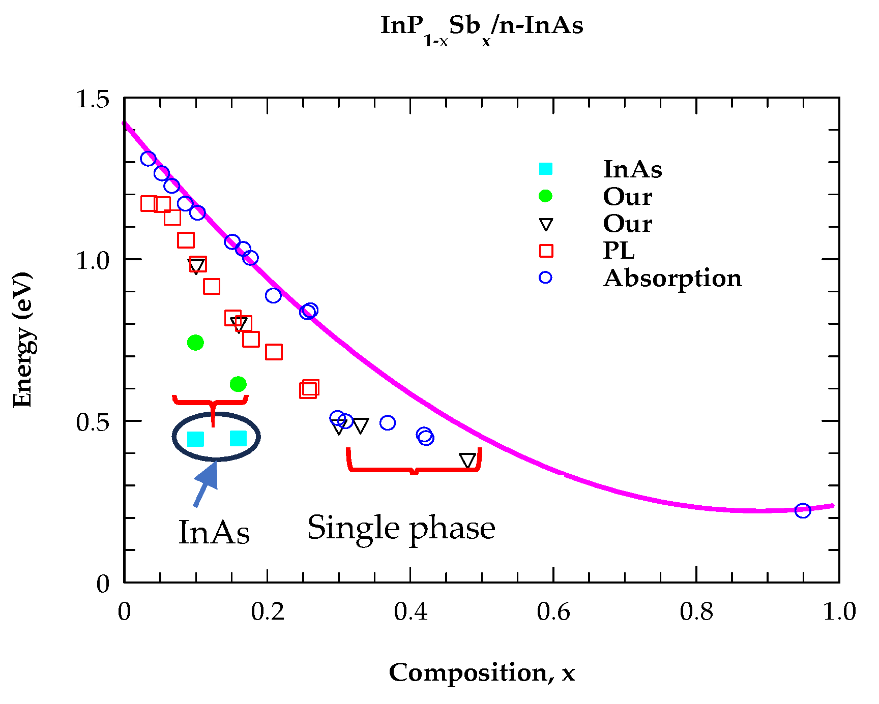
4.2. Analysis of Photoluminescence Spectra
Reihlen et al. [
26] performed low-temperature (10 K) PL and absorption measurements on several InP
1−xSb
x epilayers grown by OMVPE using InP, InAs, and InSb substrates. Large miscibility gaps were predicted [
26] from x = 0.02 to 0.97 from the second derivative of Gibb’s free energy [
32]. We have estimated the energy bandgaps
at 13 K on GS-MBE-grown InP
1−xSb
x/InAs samples having different compositions x by using a 532 nm DP-SSL excitation source. In
Table 3, the results of our PL study are included (see
Figure 6) for 0.10 ≤ x ≤ 0.48 using solid black inverted triangles, green-filled circles, and light-blue-filled squares. Comparison is made with the absorption (open blue circles) and PL data (red open square) of Reihlen et al. [
26]. Again, the x-dependent energy bandgaps (
Figure 6, magenta solid line) of ternary alloys
are calculated by adopting a second-order polynomial equation [
18]:
where
,
are the direct bandgaps of the bulk InP, InSb materials, and the term
(≡1.9) is used as a bowing parameter.
The perusal of
Figure 6 has revealed two
energy phases (small red bracket) with values displayed by black inverted triangles, green solid spheres, and a nearly constant value of InAs (substrate) shown by sky-blue-colored squares. For x ≥ 0.30, our PL study has provided only one
energy phase (large red bracket) indicated by black triangles. Earlier studies by Reihlen et al. [
26] on InP
1−xSb
x epilayers have suggested large miscibility gaps between x = 0.02 and 0.97. Our results indicated that high-quality single-phase epilayers can be obtained around x ~ 0.3 in the center of the miscibility gap. The GS-MBE-grown epitaxial layer with composition x = 0.31 is lattice-matched to the InAs substrate. The strain energy caused by lattice mismatch has locally changed the range of miscibility, making the growth of a single crystal possible. Obviously, the OMVPE results cannot be fully applied to GS-MBE-prepared InP
1−xSb
x/n-InAs samples, as the growth situation may differ from equilibrium conditions. Moreover, our MDF simulation for InP
0.67Sb
0.33 alloy provided the lowest energy gap E
0 ~ 0.46 eV, in good agreement with the existing first-principles calculation and the PL measurements.
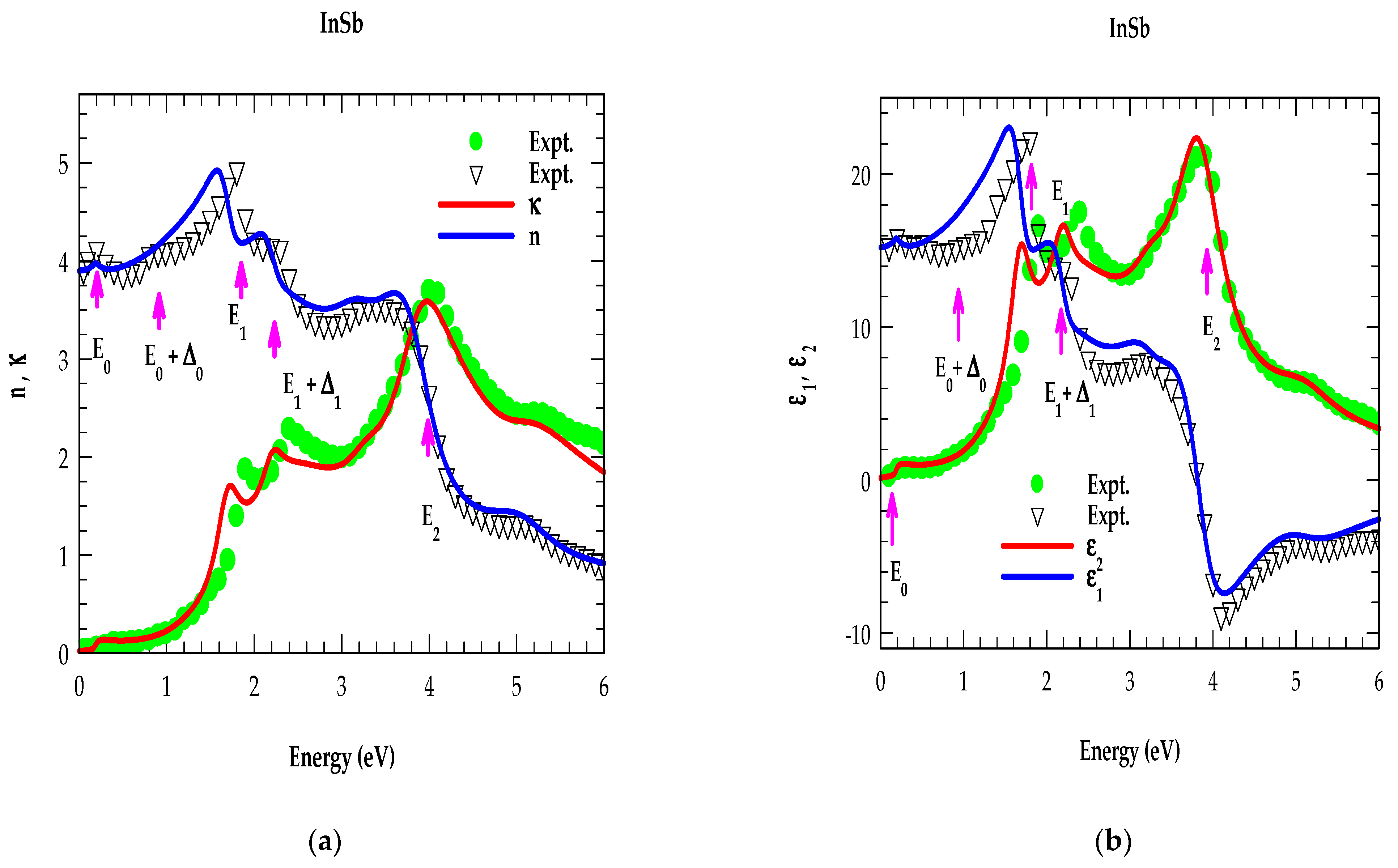
4.2.1. Analysis of Optical Constants for Binary Materials in the NIR → UV Region
Optical constants, i.e., the real and imaginary parts of pseudo-dielectric functions [
and
], are numerically obtained by using the best-fitted MDF parameters (
Table 2) following the methodology outlined in
Section 3.3. For InSb, theoretical results of
and
in the photon energy (
range are reported (red and blue lines) in
Figure 7a and
Figure 7b, respectively, and compared with the SE data of Aspnes and Studna [
22] and Seraphin and Bennett [
23] (see black and green symbols). Similar results for InP are displayed in
Figure 8a,b. The perusal of
Figure 7a,b revealed that the sharpest peaks in
are related to
transitions while in
(
), the strongest peaks are linked to
transitions.
For InSb and InP, our calculated results of reflectance
and absorption
coefficients displayed in
Figure 9a,b and
Figure 10a,b have agreed reasonably well with the experimental results [
22]. Interestingly, the simulations in each category has provided distinct CP energy features of the band structures arising from the inter-band transitions (indicated by magenta vertical arrows). Like
and
, the
and
data have also revealed appropriate shifts in the major CP energy structures. Among other features, the reflectivity
spectra indicated the strongest peaks at the
gaps, varying between ~0.6 and 0.625 [see
Figure 9a and
Figure 10a], in very good agreement with the observed values for the binary (InP, InSb) materials [
22].
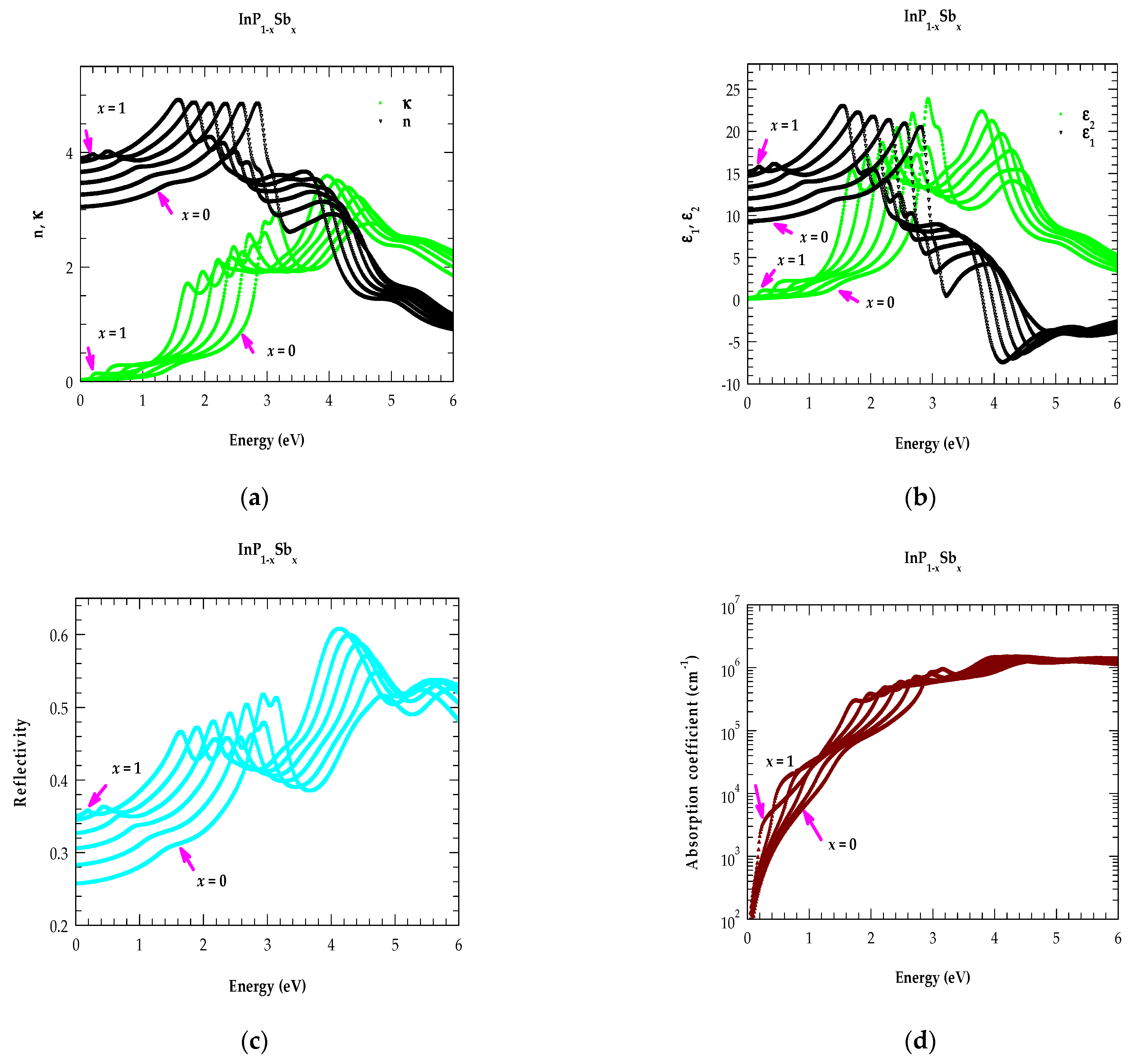
4.2.2. Analysis of Optical Constants for InP1−xSbx Alloys in the NIR → UV Region
To calculate the composition-dependent optical constants for InP
1−xSb
x ternary alloys, we have meticulously obtained MDFs from the values (
Table 2) of their binary counterparts (InP, InSb) by using appropriate quadratic expressions [
18] involving x of the major CP energies, while the strength and broadening parameters are obtained deliberating a linear dependence articulation on x [
38].
In
Figure 11a–d, we have reported our simulated results of
,
, respectively, for InP
1−xSb
x ternary alloys in the photon energy range of
by selecting the composition increment of x by 0.2. In each figure, the results have revealed an appropriate shift in the CP energies toward the low-energy side as x is increased, in corroboration with the observed changes from InP → InSb band structures. Like
;
,
(indicated by black and green points in
Figure 11a,b the near normal-incidence reflectivity
(shown by sky-blue-colored points) and the absorption coefficient
(represented by brown points) in
Figure 11c,d also revealed distinct composition-dependent shifts in CP structures. Our simulations of optical constants for the InP
0.67Sb
0.33 alloy have provided the lowest energy bandgap value E
0 ~ 0.46 eV, in very good agreement with the existing first-principles calculation as well as our PL measurements (see
Figure 6 and
Table 3).
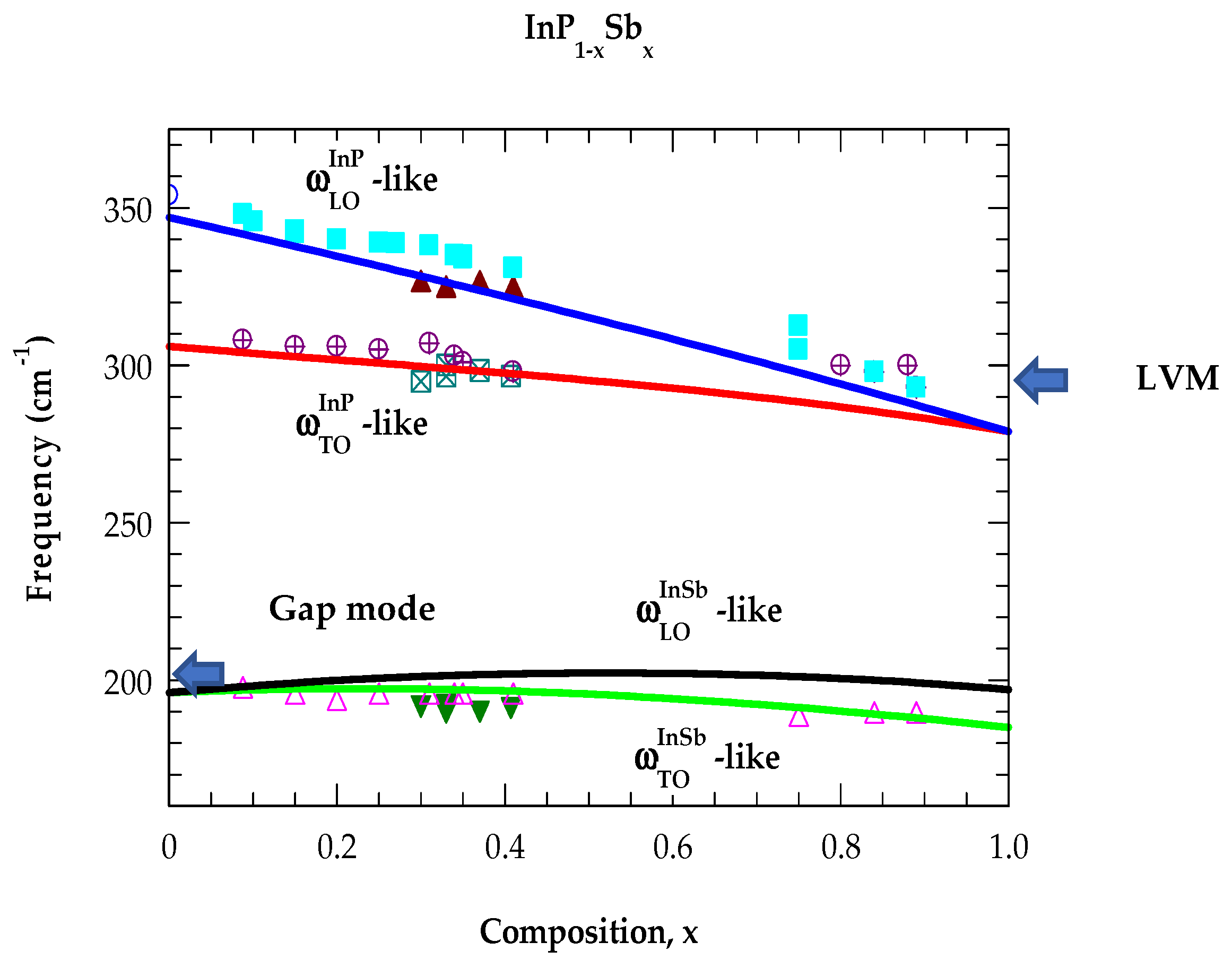
5. Concluding Remarks
In conclusion, systematic assessments of phonon and optical characteristics are achieved both experimentally and theoretically for comprehending the vibrational, structural, and electronic behavior of high-quality GS-MBE-grown InP
1−xSb
x/n-InAs (001) epilayers (0.1 ≤ x ≤ 0.48). To estimate the composition-dependent phonons, we have employed a Reinshaw InVia Raman spectrometer using a DPSS 532 nm laser as an excitation source. For bulk InP and InSb, the observed separations of (
modes are 50 cm
−1 [
48] and 8 cm
−1 [
49], respectively. In each InP
1−xSb
x/n-InAs (001) sample, our RSS measurements have identified InP-like
a DAO mode while revealing (
Figure 2) InSb-like DALA, A
1g Sb-impurity mode, and an unresolved broad optical band near ~195 cm
−1 with FWHM ~ 10 cm
−1. For x = 0.48, while the separation (see
Figure 4) between InP-like (
) modes decreases, the split in InSb-like phonons increases, but only slightly. Our calculated separation between InSb-like (
) modes stays much smaller (~3–4 cm
−1 << FWHM) than the observed broad bandwidth—thus, resolving the
mode in InP
1−xSb
x is quite difficult [
24,
25,
26,
27]. Although the observed Raman line shapes of ternary InP
1−xSb
x alloys are signified as the optical phonon density of states exhibiting two-phonon-mode behavior, no LVM (In
Sb:P; x → 1) and gap mode (In
P:Sb; x → 0) have been perceived near the limiting values of x. Our ATM-GF calculations [
59], providing accurate values of the impurity vibrational modes, have offered further support for the “two-phonon-mode behavior”. Accurate results of bandgaps are achieved using PL measurements by calibrating the radiation lines of a Xe lamp and exploiting the SPEX 500M monochromator with a 532 nm DP-SSL excitation source. Although the earlier studies [
26,
27] on InP
1−xSb
x epilayers suggested large miscibility gaps from x = 0.02 to 0.97, our careful HR-XRD and PL results on
energy gaps have indicated attaining high-quality, single-phase epilayers around x ~ 0.3, ascribed to the effect of lattice match. A complete set of model dielectric functions is methodically achieved by using Adachi’s MDF approach [
37,
38] for calculating the optical dispersion relations of both the binary InP, InSb and ternary InP
1−xSb
x alloys. For InP, InSb materials, the detailed analyses of optical constants (viz., n(E), κ(E);
,
; α(E), and R(E)) over the photon energy range 0 ≤ E ≤ 6.0 eV have exhibited reasonably good agreement with the SE experimental data [
22,
23]. The extension of MDF methodology to InP
0.67Sb
0.33 alloy has provided the lowest energy bandgap value E
0 ~ 0.46 eV, in very good agreement with the existing first-principles calculation [
18] and PL measurements. We strongly feel that our systematic study, using RSS and PL measurements along with the MDF simulations of optical constants, has provided valuable information on the vibrational and optical characteristics of InP
1−xSb
x/n-InAs (001) epilayers which can be extended to many other technologically important materials.


