Other than single junction photodetectors, the heterojunction 2D structured materials can be fabricated through van der Waals interactions [
66,
67]. Heterojunction material systems can not only combine advantages from each material [
68,
69], but also allow for the modulation of band structures for photoresponse improvements [
12]. Two-dimensional heterostructures can be classified into two main species (graphene-based and hybrid semiconductor materials) based on the material composition and physical principles.
3.1. Graphene-Based Heterojunctions
Researchers have found that responsivity of graphene-based photodetectors is greatly increased due to their extraordinary electrical and optical properties. However, the gapless nature of intrinsic graphene and the limited light absorption in each atomic layer prevent efficient photocarrier separation in graphene photodetectors. To overcome this shortcoming, the integration of graphene with other materials appears to be a promising approach [
70,
71], such as quantum dots/graphene [
72,
73], MoS
2/graphene [
12], WSe
2/graphene [
71] and Bi
2Te
3/graphene [
74] heterojunctions. One easy and functional approach for fabrication of these heterojunctions is by reattaching the different films onto each other [
12]. This multiple transferring procedure may bring contaminations to the interfaces, which would limit the practical applications. Epitaxial growth of 2D material directly onto other material layers is an alternate approach for fabricating such heterostructures [
75,
76], which enables a guarantee of the quality of the material systems. Photodetectors based on those 2D graphene-based heterojunctions have achieved unprecedented high responsivity and sensitivity because of the synergistic effects. In those systems, the graphene layers are applicable for broadband, ultrafast technologies, whereas the other semiconductors are suitable for applications requiring strong light absorption and electroluminescence.
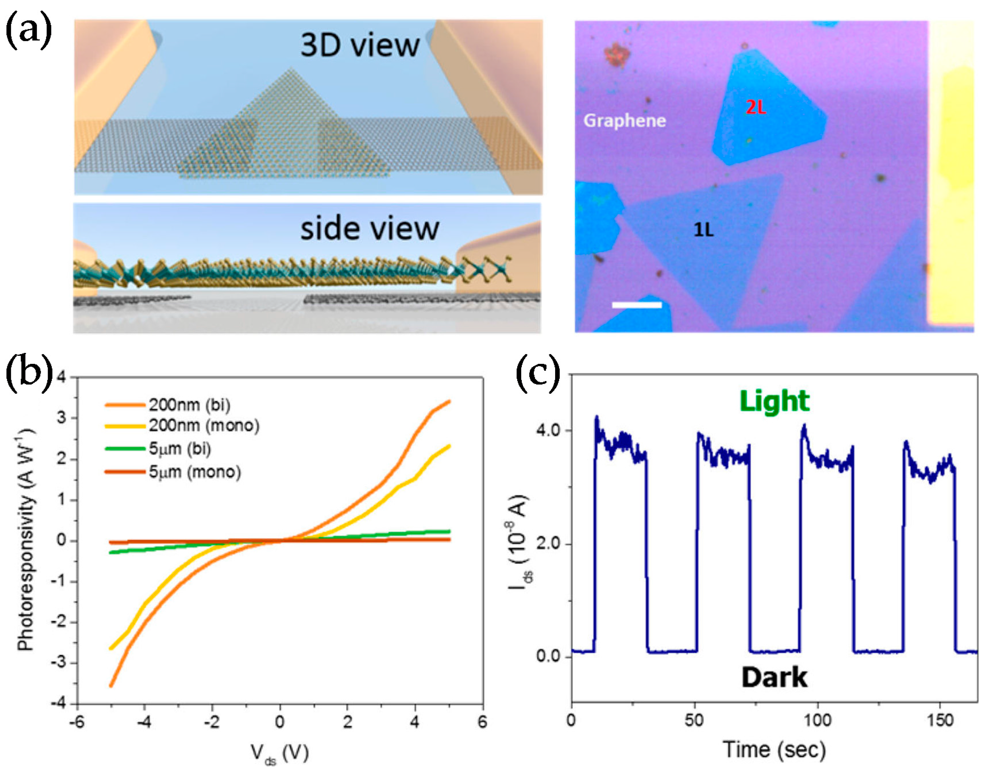
A novel hybrid graphene-quantum dot phototransistor has been fabricated by Gerasimos Konstantatos et al. [
77], as shown in
Figure 1a. Because of the strongly light-absorbing and spectrally tunable colloidal quantum dots, the responsivity of this hybrid photodetector is as high as ~5 × 10
7 AW
−1 at low excitation power and the photocurrent response obviously follows the absorption of the PbS quantum dots (
Figure 1b). This work demonstrates that efficient electronic coupling of graphene with other technologies such as light absorbing materials will open pathways for high performance photodetectors.
As a typical TMD material, MoS
2 has shown reasonably high photoresponsivity ranging from 7.5 mA W
−1 to 780 A W
−1 under ambient conditions. The bandgap of MoS
2 can be tuned by varying the number of layers in crystal structure. A tunable direct band gap would provide great flexibility for designing devices with a wide spectrum response.
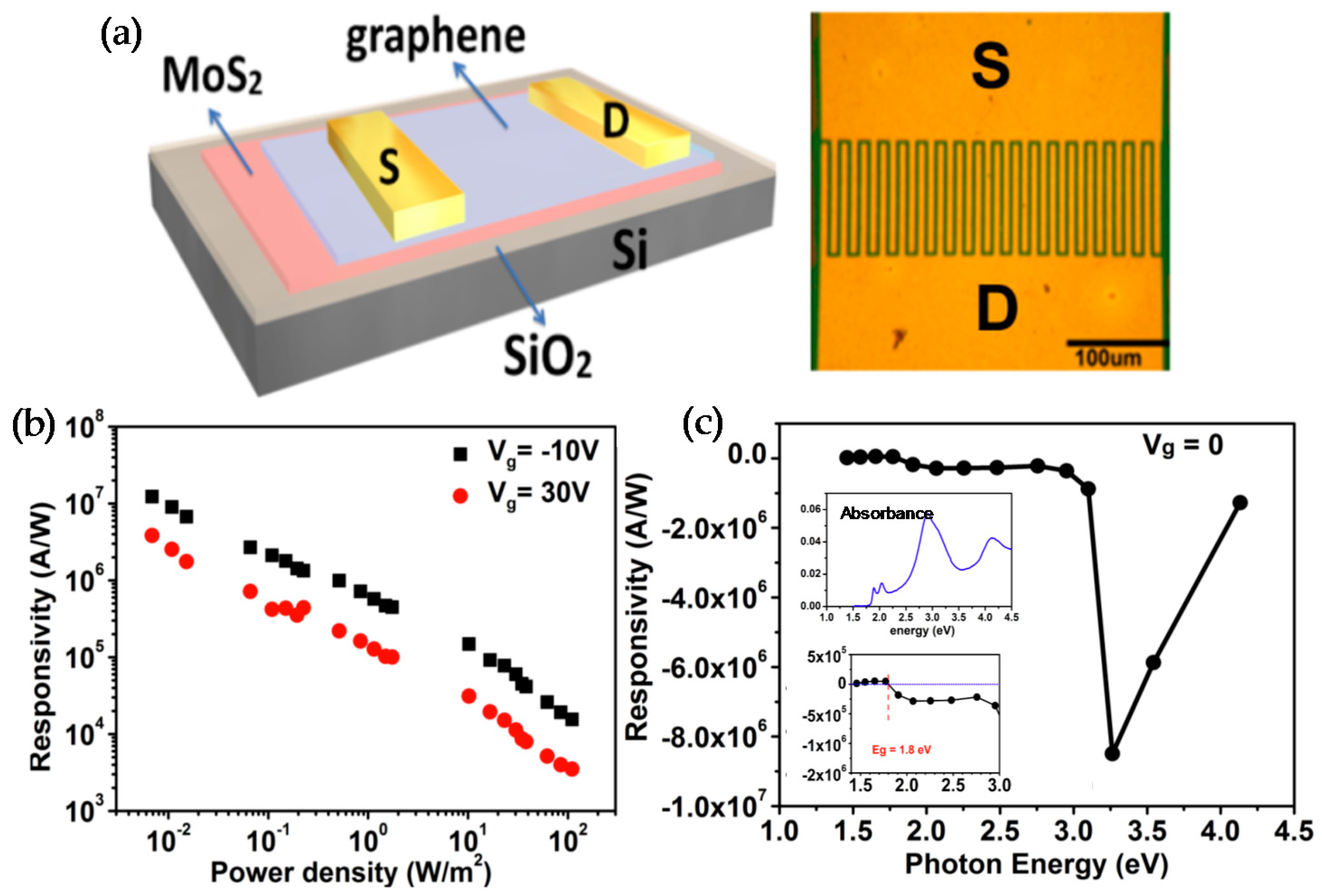
Figure 2a shows a schematic view of a photodetector based on a graphene-on-MoS
2 heterostructure, proposed by Wen**g Zhang et al. [
12]. It is worth noting that the photoresponsivity of this device reaches 1.2 × 10
7 A W
−1 (at V
g = −10 V; V
ds = 1 V; light power density ~0.01 W m
−2) as shown in
Figure 2b. The dependence of photoresponsivity of the graphene/MoS
2 heterojunction on the wavelength of light at room temperature is shown in
Figure 2c, which implies photoresponsivity is induced when the excitation energy is higher than the absorption band gap of MoS
2 (1.8 eV), which is consistent with the optical absorption feature of MoS
2 layer (
Figure 2c inset). It suggests that the photocurrent, generated in this system, originates from light absorption in MoS
2. This novel 2D heterostructure material exceeds the capacities of its constituents, providing a valuable reference for optoelectronic applications based on various heterostructural 2D materials.
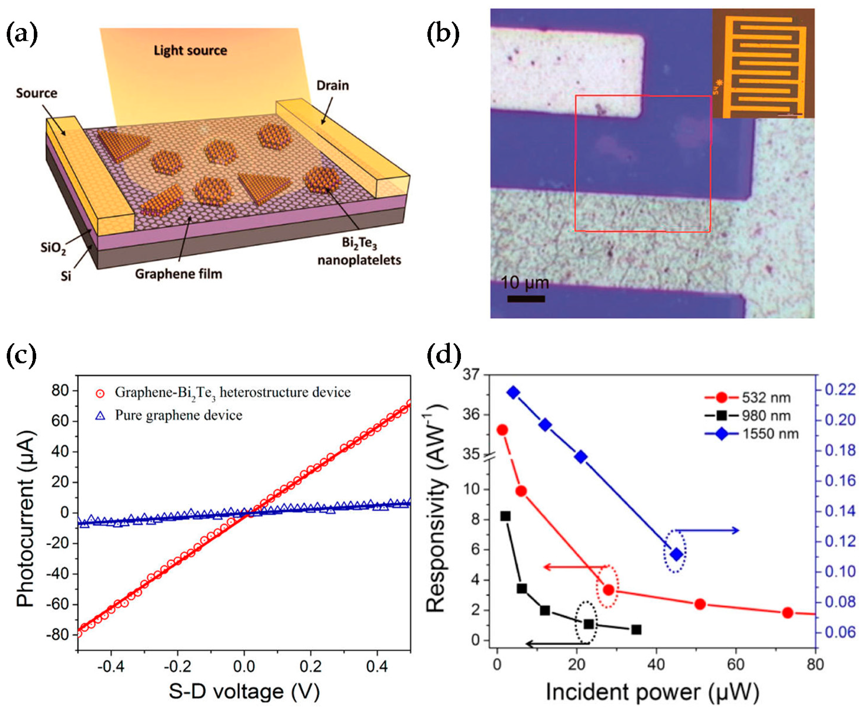
Another class of 2D materials, topological insulators, mainly Bi
2Te
3, Bi
2Se
3, Sb
2Te
3, are utilized to fabricate heterostructure materials with graphene. For example, Hong Qiao et al. has presented an effective broadband (from vis to IR) photodetector based on a graphene-Bi
2Te
3 heterostructure [
74]. Similar to graphene-based materials, the crystal structure of Bi
2Te
3 is comprised of typical layered materials via van der Waals interactions with a hexagonal unit cell. Hence, large area epitaxial growth of Bi
2Te
3 nanocrystals on graphene templates is feasible. The schematic and optical images of such heterostructure phototransistor devices are illustrated in
Figure 3a,b. For comparison, photocurrent results of two different devices based on monolayer graphene and heterostructure materials without applying the gate bias are presented in
Figure 3c. It is obvious that the photocurrent of the heterostructure device is about 10 times higher than that of the pure graphene device. From
Figure 3d, different wavelengths show high photoresponsivity which proves such heterostructured devices are capable of broadband photodetection from visible to NIR regime. The highest photoresponsivity is shown at the visible region (532 nm) (about 35 A W
−1 at an excitation power of 1.28 μW).
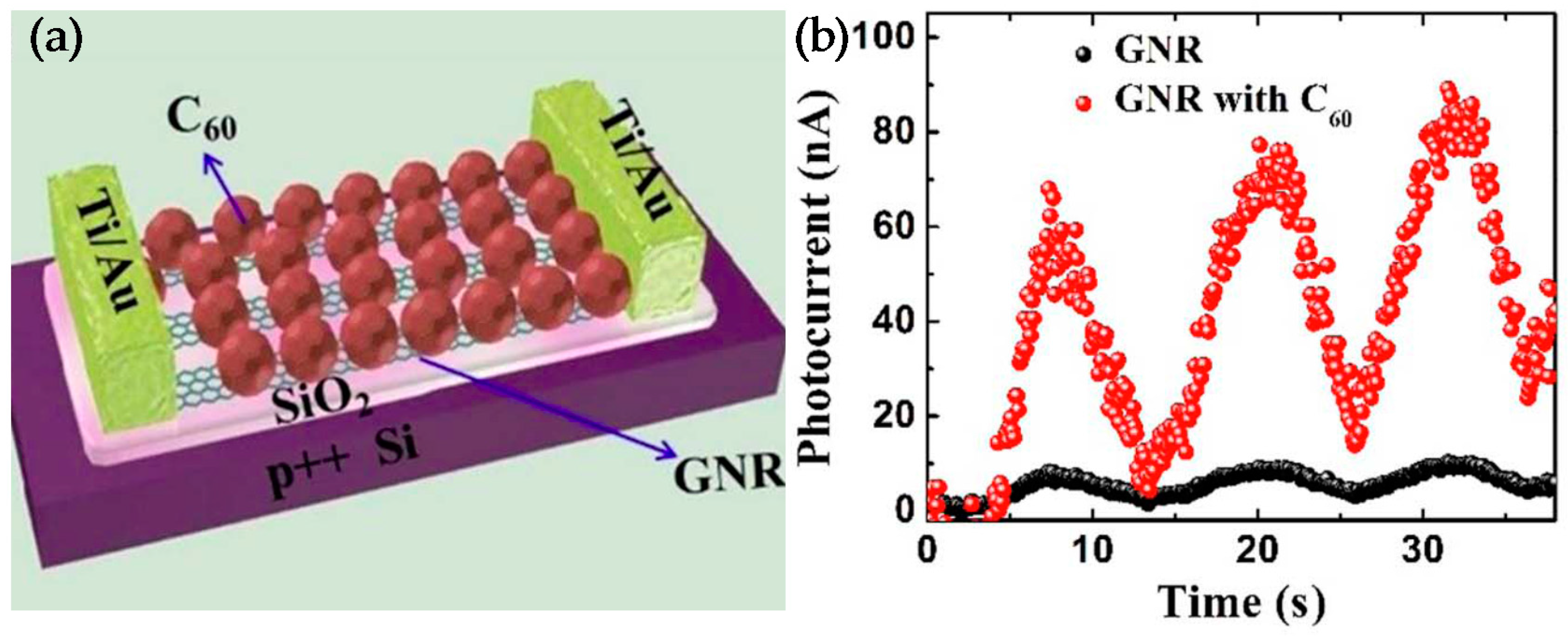
In these graphene-hybridized semiconductor systems, the light absorption mainly depends on the semiconductors, where graphene functions only as a carrier transporting layer. Hence, the broadband absorption characteristics of graphene have not been fully utilized in these heterojunctions. In order to overcome the disadvantages, graphene nanoribbons (GNRs) have been adopted to engineer the band structure of hybrid graphene photodetectors [
78]. The absorption of GNR-based phototransistors is broadband and determined by the pertinent bandgap opening in the GNR, which can be controlled by the nanoribbon width. For example, a novel photodetector has been fabricated by Xuechao Yu et al. which is composed of GNRs with fullerene (C60) film (
Figure 4a) [
79]. The photoresponse of this GNR-C60 hybrid phototransistor under global irradiation is ∼0.4 A W
−1, as shown in
Figure 4b, which is about one order higher than the bare GNR phototransistor.
3.2. Hybrid Semiconductor Materials with p-n Junctions
Besides graphene-based heterojuctions, p-n junctions provide another platform to improve photoresponse [
80]. As we know, p-n junctions are the basic building blocks of many optoelectronic devices, which have been utilized for rational control of their fundamental parameters, such as the bandgap, mobility and effective mass of charge carriers. Therefore, vertical p-n heterojunctions based on distinct layered materials have been widely used. For example, a heterojunction p-n diode based on phosphorene/monolayer MoS
2 has been fabricated by van der Waals forces [
81], which exhibits excellent current-rectifying characteristics and high I
light/I
dark ratio, up to 3 × 10
3. In addition, graphene p-n junctions [
82,
83,
84], TMD p-n junctions [
85] and BP p-n junctions [
86,
87] have been constructed and exhibited high responsivity, due to effective separations of photo-generated electron/hole pairs by internal electric fields.
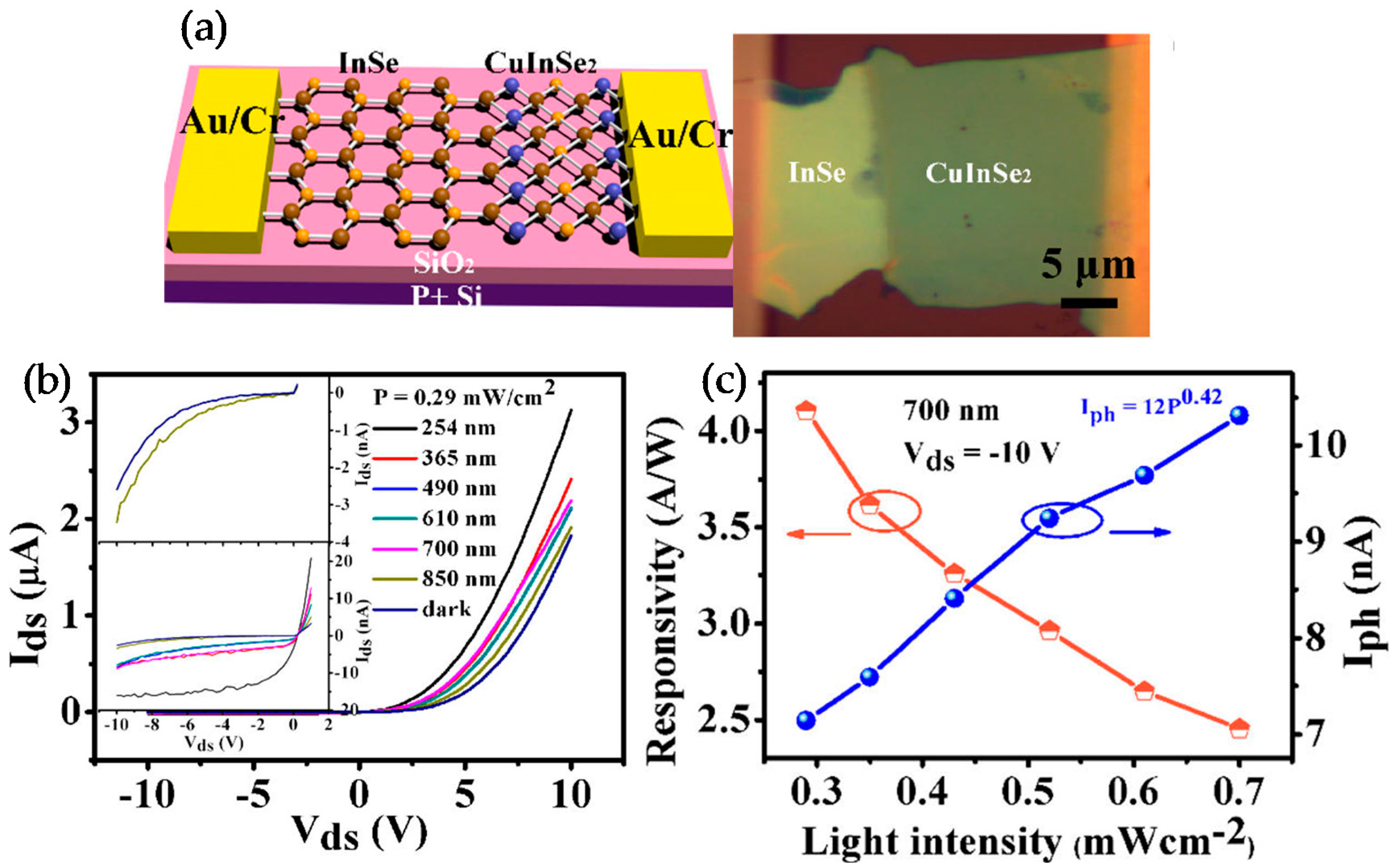
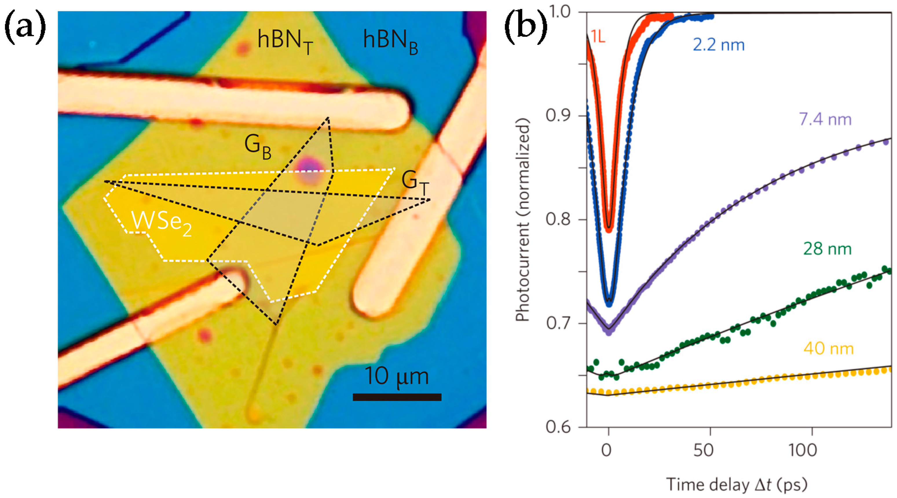
As shown in
Figure 5a, Wei Feng et al. have fabricated a lateral thin-film InSe/CuInSe
2 p-n hereojunction by a simple chemical do** procedure [
88]. This lateral diode exhibits a broadband photoresponse ranging from 254 nm to 850 nm, because of the small band gaps of InSe and CuInSe
2 (
Figure 5b). Meanwhile, a large responsivity of 4.2 A W
−1 is obtained at a wavelength of 700 nm with illumination power of 0.29 mW cm
−2 and bias voltage of V
ds = −10 V (
Figure 5c). Such excellent performance of this p-n diode is attributed to bandgap engineering by selecting desired materials and high optical absorption by increasing channel thickness.


