1. Introduction
Traditional fossil energy has to be replaced by renewable energy sources on an urgent basis due to the limited reserves and environmental pollution. Solar power has garnered significant research attention because of its clean nature, reproducibility and adequacy on our planet [
1]. Since Chapin and Pierson developed the first practical single-crystal silicon solar cells and demonstrated the practical utilization of photovoltaic technology that converts solar energy into electricity in 1954, the development of solar cell technology has been extremely rapid [
2]. At present, there are three generations of solar cells with different structures, ranging from monocrystalline silicon to nanostructured thin-film, hybrid and organic cells [
3]. The first generation mainly consists of monocrystalline and polycrystalline silicon-based solar cells. The second generation is composed of a series of thin-film solar cells, such as
α-Si, CdTe, GaAs, CIGS and CuGaSe [
4,
5]. The third-generation includes single-cell or tandem devices based on Cu
2ZnSnS
4 (CZTs), Cu
2ZnSnSe
4 (CZTSe), quantum dot solar cells, organic dye-sensitized solar cells and perovskite solar cells [
6]. Si-based solar cells have occupied the current market due to the solid foundation of long-term development [
2]. At present, the maximum efficiency of Si-based solar cells reached 31.25% in 2022. However, any significant advancement has not been achieved due to the material limitations and Shockley-Queisser (S-Q) limits [
7].
The perovskite structure has attracted worldwide attention due to its advantages, such as adjustable bandgap, rapid spectral response and solution-based processing. Since the report on initial efficiency of 3.8%, a series of pivotal problems, such as the dissolution of MAPbI
3 in liquid electrolytes and application of crucial materials (MAPbI
3 and spiro-MeOTAD), perovskite solar cells have seen an exciting era of rapid development [
8]. The efficiency of perovskite-based single-cell increased from 3.8% in 2009 to 25.7% in 2022. Such a rapid increase in conversion efficiency is conducive to the replacement of Si-based solar cells with perovskite solar cells [
9].
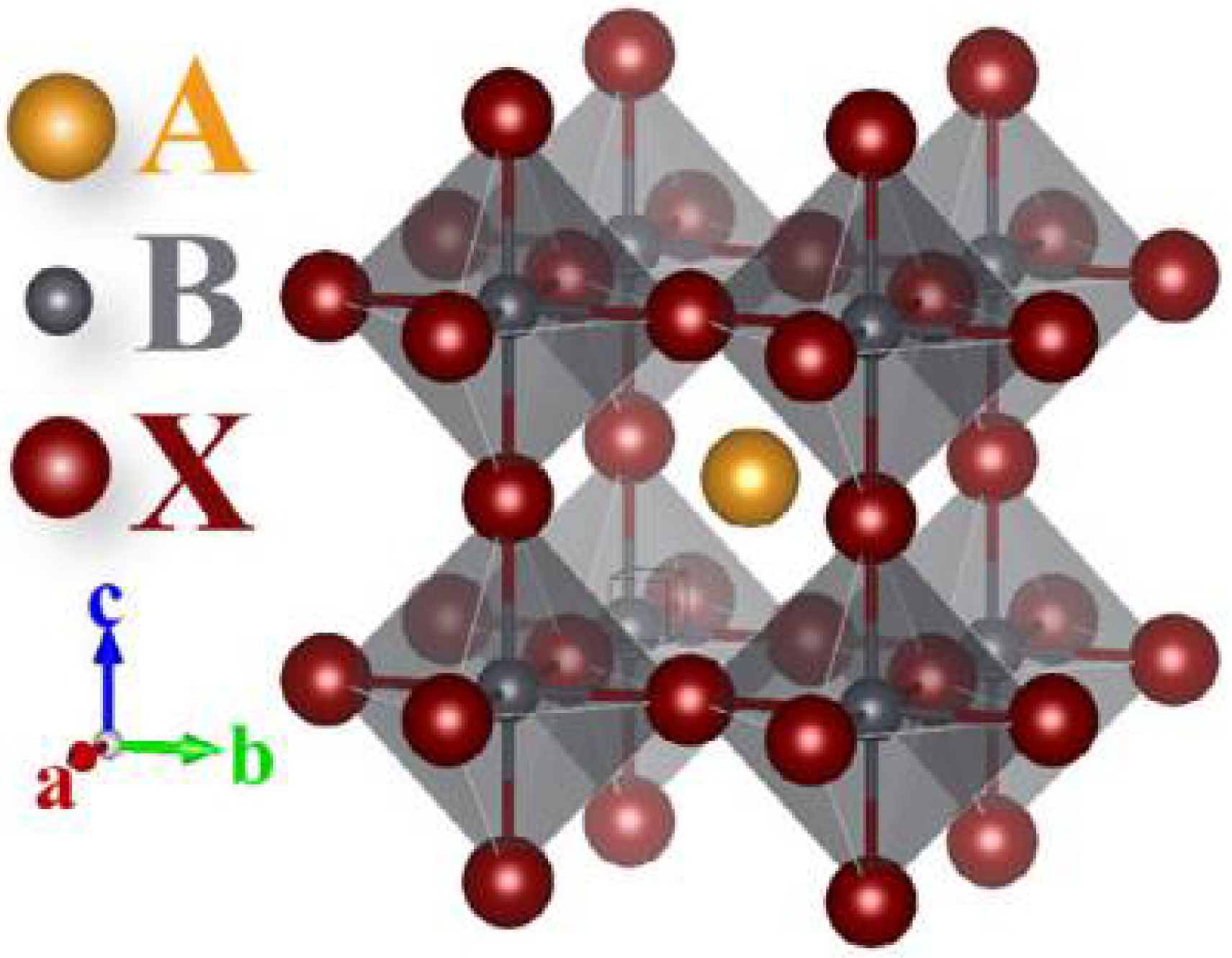
Halide perovskites usually possess a 3D structure [
10], as shown in
Figure 1, with a chemical composition of ABX
3, where A represents large-sized cations (CH
3NH
3 (MA
+), formamidinium (FA
+) and cesium (Cs
+)), B refers to the divalent metallic cation and X denotes the halide anion (Cl, Br, or I) [
11].
Despite the rocketed improvement in power conversion efficiency (PCE) of perovskite solar cells, the instability of the perovskite structure impedes the commercialization of perovskite solar cells (PSCs), which is mostly caused by the presence of erratic organic cations and degradation due to water, light and oxygen [
13]. To solve these instability problems, the researchers have adopted different strategies, such as do** and interface engineering [
14]. Meanwhile, the hysteresis of J-V curves can be attributed to charge carrier accumulation in the depletion layer or neutral region of the junction, the existence or formation of defect states, and ionic migration, leading to numerous defects, such as inaccurate I-V measurements and wrongly estimated efficiency values [
15]. These phenomena have been observed in different photovoltaic architectures and perovskite solar cells.
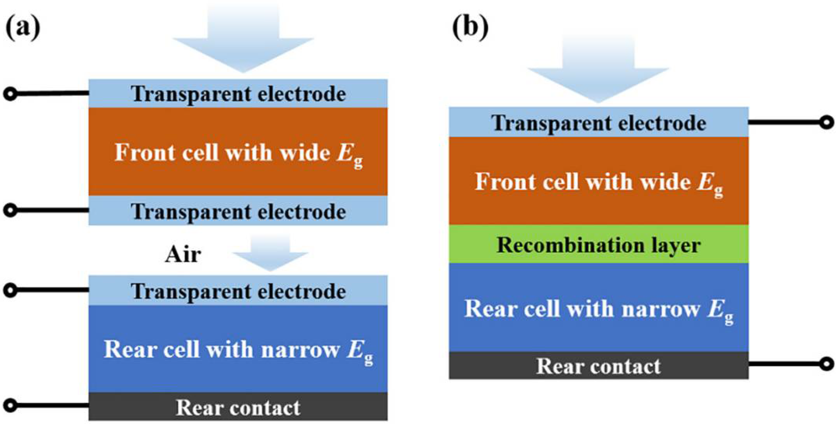
Although the efficiency of a single solar cell continues to increase, it is still difficult to achieve further breakthroughs due to the S-Q limit [
16]. At present, tandem cells, where single cells are connected in series, are utilized to break the S-Q limit [
17]. The basic principle of a tandem solar cell is shown in
Figure 2. It uses sub-cell materials with different bandgaps to absorb light in different wavelength ranges, thereby increasing the absorption range of the spectrum and effectively increasing the open-circuit voltage [
18]. Owing to the adjustable bandgap, perovskite is an ideal material for making top or bottom cells of the tandem solar cells. The bandgap can be adjusted by do** different elements. For example, increasing the proportion of Br in ABBr
3 can increase the bandgap, and increasing the proportion of Sn at the B-site can reduce the bandgap by about 1.18–2.3 eV [
19]. There are two basic structures of perovskite cells, i.e., two-terminal (2T) stacked solar cell and four-terminal (4T) stacked solar cell [
20].
Correspondingly, the hole transport layers and electron transport layers also play an important role in determining the device efficiency, which is influenced by the charge extraction and charge transportation characteristics [
22].
In addition to the PCE and toxicity, large-scale fabrication and stability should also be considered in terms of commercialization [
23]. To improve the practicality of PSCs, a vast research effort has been carried out, resulting in a large number of research articles and patents. In this review, we collect and present recent research findings, mainly about the halide PSCs, tandem structure hole transport and electron transport layers.
3. Transport Layers
In general, the configuration of perovskite solar cells is a sandwich structure, which includes an active layer that absorbs light, a
p-type hole transport layer and an
n-type electron transport layer [
40]. As a large number of carriers originate from the active layer, the photocurrent of the solar cell is greatly reduced if these carriers are not efficiently transported. Therefore, it is necessary to utilize the electron transport layer and hole transport layer to timely separate the photo-generated carriers in the active layer [
41]. Hence, the material and structure properties of the electron transport layer and hole transport layer influence the construction of high-performance perovskite solar cells.
An excellent electron/hole transport layer possesses good light transmittance, selective carrier separation and stability under light, heat and humidity. At present, the widely used transmission layer structures are mainly planar and mesoporous. The commonly used electron transport layer materials are mainly copolymers and metal oxides, such as PCBM, BCP, ZnO and TiO
2. The hole transport layer materials are mostly composed of metal oxides and polymers, including Spiro-OMTED, PTAC, PTAA and NiO
x [
42].
3.1. Design of Electron Transport Layer
Chen et al. have synthesized nanocrystalline WO
x as an electron transport layer using an ultra-low temperature (50 °C) solution-based process, which effectively avoided several problems, such as the high defect density of WO
x. The power conversion efficiency of the resulting perovskite solar cell reached 20.77% [
43].
Huang et al. have utilized SnO
2 as an electron transport layer in flexible PSCs and studied the influence of ETL thickness by adjusting the concentration of SnO
2 [
44]. It has been concluded that the optimal ratio of SnO
2 is around 5%. The results revealed that the SnO
2 improved the surface properties between the perovskite layer and electron transport layer, reduced the density of defect states and enhanced the absorption capacity perovskite layer. The AFM images of as-synthesized SnO
2 on a flexible substrate and the corresponding transmission and reflection spectra are shown in
Figure 5. The flexible solar cell, with the structure of polyethylene 2,6-naphthalate(PEN)/ITO/SnO
2/perovskite/Spiro-OMeTAD/Ag, could finally achieve a PCE of 19.51% and maintain 90% of the initial PCE after 6000 cycles.
Jiang et al. have found that the incorporation of F8BT (poly(9,9-dioctylfluorene-co-benzothiadiazole)) into PCBM could solve the long-standing problems of poor film formation and inferior electronic mobility of PCBM [
45]. F8BT is an optoelectronic polymer with excellent film-forming properties and exhibits better electron mobility than hole mobility. Therefore, F8BT can improve the performance of PCBM. Jiang et al. have reported that the addition of only 5 wt % F8BT could decrease the roughness of both PCBM and active layers [
45]. Consequently, a solar cell, with a structure of Ag/PCBM/BCP/perovskite/NiO
x/ITO, has been fabricated and demonstrated that the optimal amount of F8BT could significantly increase the IPCE, PCE, carrier concentration and EQE. The electrical impedance spectroscopy revealed that the addition of F8BT improved the device’s ability to separate electrons and holes and reduced the dark current. Li et al. have pioneered the production of uniform and compact TiO
2 layers using the gas pum** method, which is usually called gas-phase quenching [
46]. This thin, compact, pinhole-free TiO
2 can also improve the crystalized quality of perovskite material and enhance the power conversion efficiency. Compared with conventional drying, the PSCs with gas-phase quenching exhibit high PCE (>20%), originating from the high short-circuit current density (J
SC). Moreover, the as-fabricated device rendered high stability and retained 66% of the initial PCE after 550 h. On the other hand, the PCE of the device, which has naturally dried TiO
2, is rapidly decreased in only 200 h under a humid environment (RT 40−60%). Meanwhile, this device with gas pum** TiO
2 exhibits great potential for large-area applications. Yang et al. exploit a nanopatterned mesoporous TiO
2 as ETL by the nanoimprinting method for nanopatterning [
47]. They found that the PSC with 127 nm mesoporous TiO
2 film could reach the highest PCE of about 15.83%. Cao et al. utilized the TaCl
5 doped SnO
2 as ETL in the n-i-p structure PSC [
48]. After adopting TaCl
5 doped SnO
2 ETL, the open circuit voltage is increased from 0.97 to 1.08 V, and the PCE is increased from 16.38% to 18.23%.
3.2. Design of Hole Transport Layer
Until now, a large number of studies about different organic hole transport materials, such as Spiro-OMeTAD, PTAA and PEDOT:PSS, have been carried out to improve the efficiency and charge extraction. However, the development of various hole transport materials is expensive and leads to instability. On the other hand, a series of inorganic KTL materials, such as NiO, CuO, CuI, VO
x, CuCrO
2, CuGaO
2, MoO
x (as an interlayer), and WO
x, are also considered due to their low cost, abundance and non-toxicity [
49,
50,
51].
For small-molecule polymers, polyaniline (PANI) is an attractive photovoltaic material because of its excellent performance and low cost. Recently, Bourdo et al. have proposed that PANI could be doped with lignin sulfonic acid and camphor sulfonic acid to tune the work function and processed with DMSO to obtain LS-PANI-CSA. The introduction of LS-PANI-CSA as an HTL of an inverted perovskite solar cell decreases the interfacial roughness between the perovskite layer and HTL. At the same time, this structure can enhance the adhesion and dispersion of perovskite. Meanwhile, the interstitial spaces of the perovskite become smaller, and the obvious pinholes are not observed. After the experiment, the research team found that the utilization of LS-PANI-CSA HTL, with a thickness of 15 nm, could achieve optimal performance [
52].
Moreover, carbon quantum dots, as a newly emerging optoelectronic material, are also being widely studied. Kim’s group has indicated that the combination of carbon QDs with NiO
x could effectively reduce the J-V hysteresis loop, enhancing the stability of PSCs [
53]. At the same time, this structure can improve the carrier transmission capacity and increase the short-circuit current and fill factor (FF). The PCE of the PSC with QDs/NiO
x as an HTL was found to be 17.02%, which is significantly higher than the PSC with NiO
x as an HTL (15.66%). Moreover, the PSC with QDs/NiO
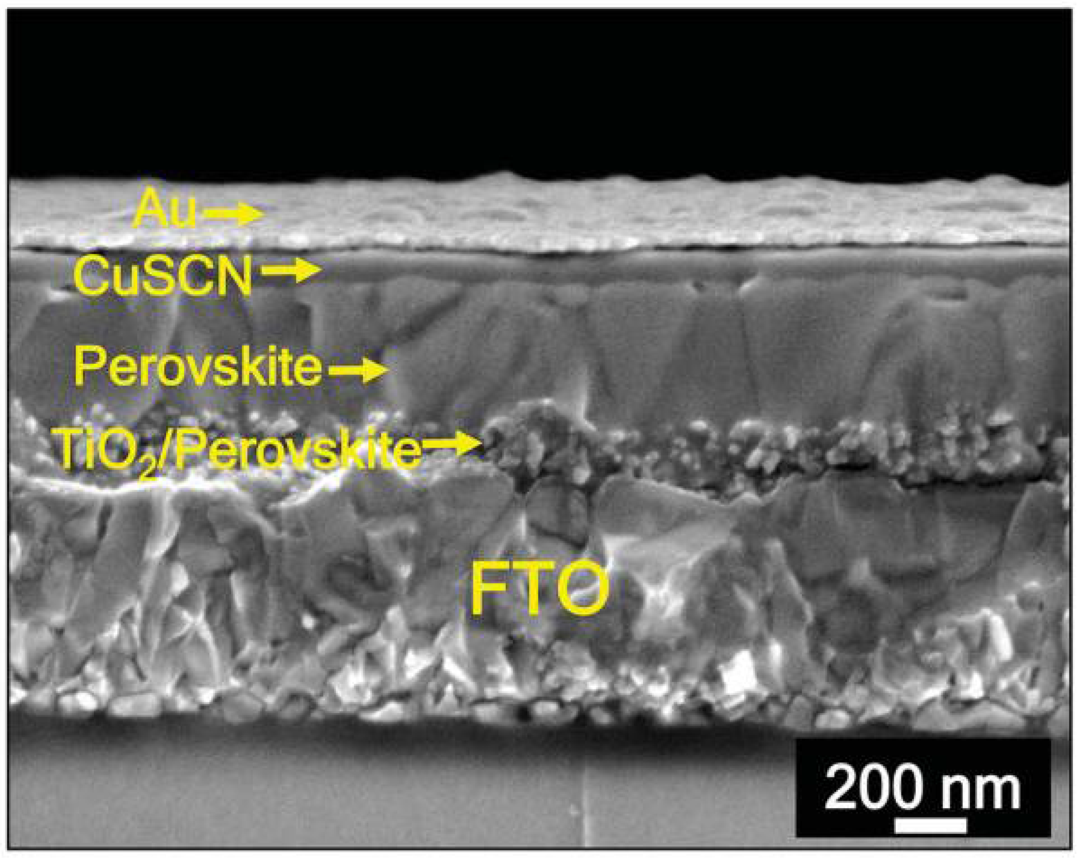
x as an HTL was left in the air for 190 h and retained 70% of the initial PCE. Milic et al. have demonstrated that CuSCN could be used instead of traditional Spiro-OMTED as a perovskite HTL due to its excellent hole transport capacity, thermal stability, solution-based processing and cost-effectiveness [
54]. After a series of experiments, it has been reported that the PCE of PSC with CuSCN exceeded 20% and the device demonstrated excellent thermal stability. After covering the CuSCN with another layer of reduced graphene oxide (rGO), the operation stability of the device has also been greatly improved, and it reached 95% of the initial PCE after 1000 h operation at 60 °C. The structure of the device is presented in
Figure 6.
Furthermore, Li et al. have successfully synthesized a well-dispersed NiO
x nanometer micelle solution with oleic acid (OA) to modify the dispersion of NiO
x [
55]. This nanometer micelle solution was introduced into the Spiro-OMTAD solution to fabricate a NiO
x/Spiro hole transport bilayer. They have demonstrated that the hole transport bilayer possesses a higher hole transport rate and better stability than the pure Spiro because NiO
x played an important role in improving the passivation and surface morphology of the perovskite layer. As a result, the device with a hole transport bilayer exhibited better performance than the Spiro-based PSC. Bogdanowicz et al. have used the4,4′-((1E,1′E)-((1,2,4-thiadiazole-3,5-diyl)bis(azaneylylidene))bis(methaneylylidene))bis(
N,
N-di-p-tolylaniline) (bTAThDaz) as the HTM. bTAThDaz can tune the HOMO-LOMO energy level to optimize the performance of perovskite solar cells. The PSC conversion efficiency of their fabricated structure of FTO/TiO
2/perovskite/bTAThDaz/Ag reached 14.4% [
56]. In summary, device efficiency can be improved by using different electron/hole transport materials or by modifying the transport layer.
4. Configurations of Perovskite Solar Cells
The structure of the PSC device is usually compared with the traditional dye-sensitized solar cells, which utilize an iodine-containing electrolyte as an HTL [
57]. However, the device structure is close to the solid-state dye-sensitized solar cells because PSCs contain solid-state hole transport materials. To date, a variety of device structures have been proposed for perovskite solar cells [
58]. The main structures of a single-cell PSC are mesoporous structure and planar structure. The main feature of the mesoporous structure is the introduction of semiconducting or insulating nanoparticles to assist electronic transport or perovskite film formation [
59]. In the planar structure, the perovskite film is directly prepared without the introduction of a mesoporous skeleton, thereby making the perovskite preparation method more diverse and relaxing the constraints of fabrication conditions. Moreover, there are special device structures, such as hole-free transport structures, to simplify the process and reduce the production cost [
60].
The basic structure of the tandem PSCs is briefly introduced in the first part (
Figure 2) and it is mainly divided into two types: two-terminal tandem cells and four-terminal tandem cells. The manufacturing process of the four-terminal tandem cells is simple and does not require an additional active layer, but the two sub-cells are connected separately [
21,
61,
62,
63]. Hence, the utilization of four electrodes is easy to cause leakage current loss, and the manufacturing process becomes more complicated. For two-terminal tandem cells, the intermediate layer must have a certain degree of transparency and good electrical conductivity. This results in high requirements on the roughness, deposition temperature and solvent even though only two electrodes are involved in the intermediate layer [
64]. It is worth noting that the selection of perovskite material for top and bottom cells is based on a bandgap.
4.1. Tandem Perovskite Solar Cells
Garcia-Camara’s group has incorporated a nanostructured layer, called a super-surface layer, into the perovskite layer, as shown in
Figure 7, to introduce long-wavelength photons into the silicon bottom cell layer and disperse short-wavelength photons in the perovskite layer, resulting in improved absorption efficiency and power conversion efficiency of the PSCs. They have also introduced an antireflection layer to further reduce the loss of sunlight during the absorption process [
65]. In addition to the incorporation of LiF or MgF antireflection layers on the surface of top cell, there are several ways to increase the transmitted light. For example, Hossain et al. have utilized a self-textured ZnO as an electron transport layer, which could also act as an antireflection coating and greatly reduce the processing cost [
66]. Qiu et al. have directly used hydrogenated heterojunction silicon nanocrystals to embed an antireflection layer between perovskite and Si layers, increasing the light transmission and reducing the reflection. The final short-circuit current density reached 0.82 mA cm
−2 [
67].
Sahli et al. have directly constructed a fully textured perovskite-Si two-terminal tandem solar cell, which owns a high short-circuit current by increasing the sunlight absorption, reducing the absorption loss [
69]. This structure differs from the conventional textured perovskite-Si solar cells because its structure is completely pyramid-shaped. First, both sides of Si were etched using KOH and, then, PECVD was employed to evaporate Si nanocrystals as an intermediate transport layer instead of ITO. This effectively reduced the deposition of the Spiro layer on the texture and reduced the leakage current caused by ITO deposition. Subsequently, a Spiro layer was evaporated, and a perovskite layer was formed using the spin-coating method. Then, an SnO
2 layer and an IZO layer were formed using atomic layer deposition (ALD) and sputtering, respectively. Cai et al. have placed dielectric nanovertebras on the top of the solar cell and deposited silver nanoparticles on the bottom of the solar cell to increase the light absorption. The simulation results revealed that such a structure increases light absorption by 12.5% [
70]. Manzoor et al. have also utilized textured structures to increase light absorption and employed the polydimethylsiloxane (PDMS) polymer to attain the desired texture; the PDMS polymer was placed on the surface of a silicon heterojunction to enhance light absorption [
71].
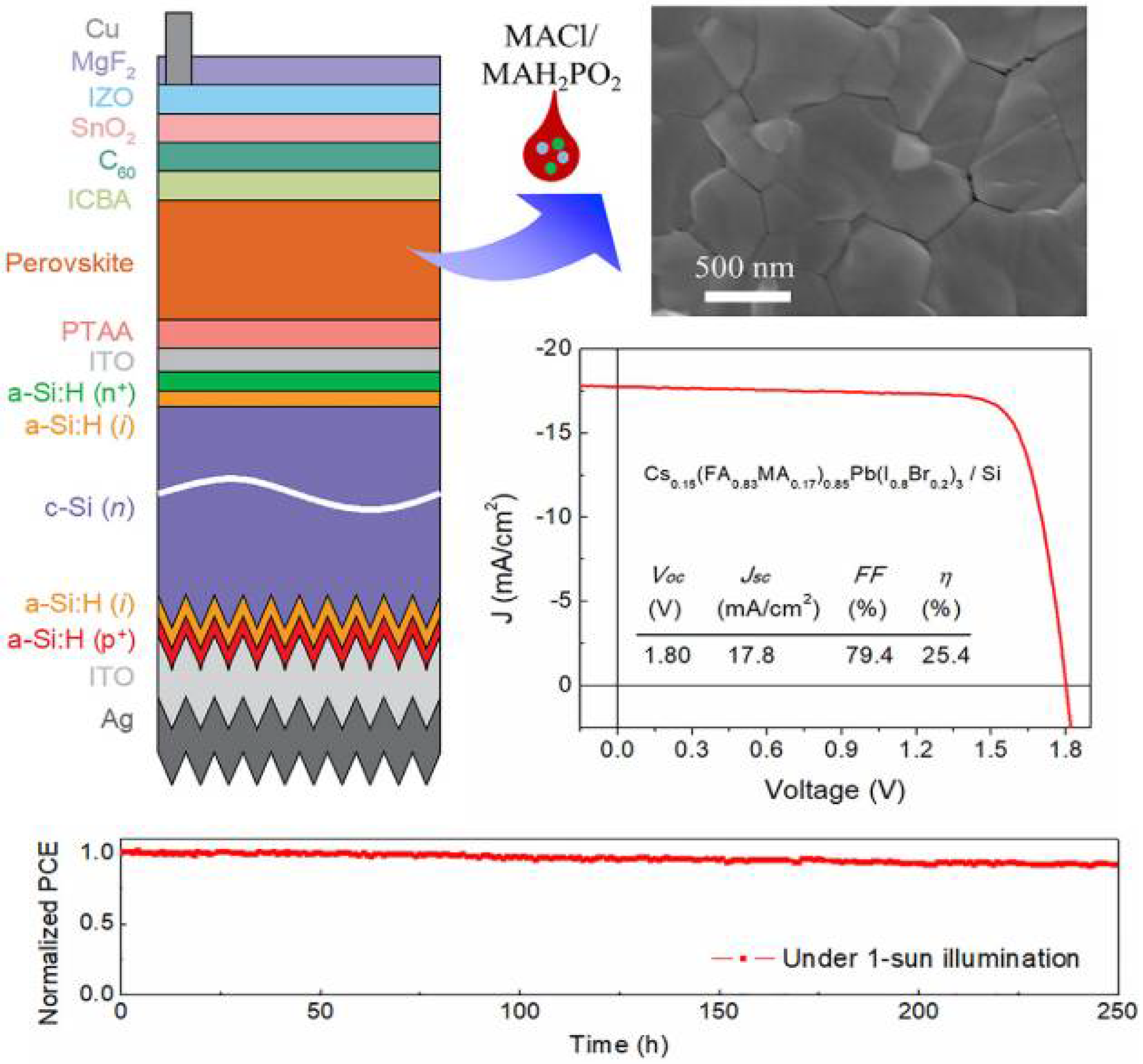
Chen et al. have improved the crystal quality of the wide-gap perovskite material by adding MACl and MAH
2PO
2 into Cs
0.15(FA
0.83MA
0.17)
0.85Pb (I
0.7Br
0.3)
3 (E
g = 1.64 eV) [
72]. These additives can increase the lattice constant and effectively reduce the density of defect states of perovskite. In the resulting device, the main role of MACl was to increase the crystalline size, and the main role of MAH
2PO
2 was to reduce defects and increase the stability of MACl after annealing. After do**, the power conversion efficiency of a single-cell solar cell reached 19.3%. In addition, the PCE of the two-terminal tandem solar cell which has the textured silicon bottom cell was as high as 25.4%. At the same time, the tandem cell still exhibited excellent stability. At room temperature and under standard sunlight, the PCE of the tandem solar cell is not reduced, even after 250 h. The structure and specific performance of the solar cell are shown in
Figure 8. They have also utilized double-sided alkylamine groups to passivate MAPbI
3, which greatly improved the thermal stability and humidity stability of the PSCs as well as increased the carrier lifetime from 278 to 889 ns [
36].
Bush et al. have employed Cs
+ cations to partially replace the FA
+ cations and fabricated a Cs
0.17FA
0.83Pb(Br
0.17I
0.83)
3-based single solar cell. Compared with MA-based solar cells, the stability has been greatly improved [
73]. Under the relative humidity of 40% and at a temperature of 35 °C, the solar cell maintained a high PCE even after 1000 h. They have also fabricated a serially connected two-terminal tandem solar cell and demonstrated a PCE of 23.6%. Tong et al. have added GuaSCN into (FASnI
3)
0.6(MAPbI
3)
0.4 to significantly improve the surface flatness, crystallinity and spectral absorption of the Sn-Pb perovskite cells [
74]. After the addition of 7 wt % GuaSCN, the optimal performance of Sn-Pb perovskite cells has been achieved with a minimum density of defect states. Moreover, the PCE reached 20.5%, and the short-circuit current was as high as 30.5 mA cm
−2. The power conversion efficiency of the four-port tandem solar cell, where the GuaSCN-based cell was serially connected with a bottom cell (1.25 eV), reached 23.4%. Min et al. have utilized an FA and MA mixture to prepare a double-cation hybrid perovskite (FAPbI
3)
0.95(MAPbI
3)
0.05 solar cell [
35]. One should note that a small amount of FAPbI
3 was used to stabilize the structure and increase perovskite stability, rendering a power conversion efficiency of 23.73%. Overall, the fabrication of tandem cells is a hopeful way to break through the S-Q limit.
4.2. HTL/ETL-Free Perovskite Solar Cells
To ensure the effective separation of excitons, whether it is an n-i-p forward perovskite solar cell or a p-i-n reverse perovskite solar cell, there are complete electron transport layers and hole transport layers on both sides of the perovskite. Although the current cost of perovskite materials is relatively low and the cost of device fabrication and ETL can be controlled, the cost of hole transport layers, such as Spiro-OMeTAD, greatly increases the cost of PSCs. As perovskite possesses hole transport properties, Etgar et al. have employed perovskite as HTL and a light-absorbing material. The power conversion efficiency of the resulting device was found to be 5.5%, which proved the feasibility of HTL-free PSCs [
75]. Moreover, the device performance was further improved by optimizing the surface morphology, and the PCE exceeded 10% [
76].
Ding et al. have used an rGO-doped carbon electrode to replace the traditional hole transport layer and fabricate HTL-free perovskite solar cells [
77]. They have incorporated a certain amount of NiO into rGO to match the energy level between perovskite and carbon electrode, thereby improving the power conversion efficiency of solar cells. Yang et al. reported that the PbTiO
3 ferroelectric layer could be inserted between the electron transport layer and perovskite layer to fabricate HTL-free PSCs [
78]. The ferroelectric layer generates a polarization field between the electron transport layer and perovskite layer. The direction of the polarization field is consistent with the direction of the built-in electric field, which effectively promotes the separation of electrons and holes. The PCE of the corresponding HTL-free PSC reached 16.37%, and the operating principle is schematically illustrated in
Figure 9.
Huang et al. have introduced a thin polar non-conjugated small-molecule electrolyte layer to modify the ITO layer and obtain ETL-free PSCs with a low hysteresis loop [
79]. The role of the small-molecule electrolyte layer as an additional layer to adjust the work function (WF) of ITO has been confirmed. Overall, the photovoltaic properties, such as PCE, hysteresis, J
sc, V
oc and FF, are enhanced due to the better alignment of energy levels. As a result, the PCE of the modified device reached 20.55%, which is much higher than the ITO-based ETL-free device (12.81%) and comparable to the PSCs with a conventional structure. Fan et al. have in situ prepared and incorporated AgI QDs into the perovskite material to fabricate an HTL-free PSC with high performance [
80]. They have demonstrated that an MAPbI
3:AgI (QDs) cross-blended structure deprived of AgI QDs and perovskite could be observed. There are several positive effects of AgI QDs, including better crystallization, fewer defects, and excellent distribution of Fermi level/work function (WF) between the perovskite layer and ITO layer.
Similarly, Cheng et al. have designed, synthesized and utilized hydroxylethyl-functionalized imidazolium iodide ionic liquid to modify FTO [
81]. It has been reported that the ionic liquid could successfully decrease the surface potential and WF of FTO, thereby efficiently blocking the diffusion of holes and optimizing the alignment of energy levels. Consequently, the PCE of corresponding PSC increased from 9.01% to 17.31%, and the stability and hysteresis were also improved. HTL/ETL-free PSCs are a novel and cost-effective structure that deserves further research.
4.3. Perovskite Solar Cells and Graphene
Graphene is an excellently honeycomb-structured material, which has garnered much attention in optoelectronic devices, such as OPVs, LEDs, OLEDs and photodetectors, because of its unique physical, chemical and mechanical properties as well as extraordinary thermal, electronic and hydrophobic properties [
82]. Moreover, graphene oxide derivatives can be processed in a solution state [
83]. In PSCs, graphene is mainly used as a barrier layer to impede the degradation of the perovskite layer and HTL due to its high hole transport velocity and low resistance [
84]. Hence, the utilization of graphene in PSCs has also been widely studied.
Lee et al. have utilized an improved method to transfer the graphene layer instead of conventional copper-based etching [
85]. The CVD-synthesized graphene can form better contact with the perovskite layer. They have introduced three layers of impermeable graphene with atomic thickness as an interfacial barrier to obstruct moisture, I-ions and Au diffusion. Owing to the high hole mobility, the PSC device with Au, CuSCN, graphene (3 layers), a perovskite layer, PTAA and FTO exhibited a negligible change in PCE (15.2 to 15.8%) and a significant increase in moisture resistance. The graphene layer significantly reduced the moisture intrusion, and the corresponding device maintained > 94% of the initial PCE under 50% RH for 30 days. Similarly, Guo et al. have employed rGO as an additive in Spiro-OMeTAD HTL of PSCs to impede the diffusion of Li
+ from Li-TFSI [
86]. They have indicated that the Li
+ ions bring high hygroscopicity, which can exacerbate the degradation of the Spiro-OMeTAD HTL layer and perovskite layer. Therefore, rGO can effectively improve the stability of PSC and PCE due to its hydrophobic behavior and excellent conductivity. As shown in
Figure 10, the presence of rGO in the Spiro-OMeTAD layer effectively obstructs the diffusion of Li
+ ions, thereby improving the efficiency and stability of this device.
Sahin et al. have utilized two different amine sources, i.e., dihexylamine (DHA) and 2-ethylhexylamine (2EHA), to modify graphene oxide (GO) [
87]. Then, GO and modified GOs (mGOs) were inserted between the halide mesoporous perovskite layer and hole transport layer as a buffer layer. The device with mGO exhibited much better surface morphology and photovoltaic performance than the GO-based device. The increase in electronic transport of the samples with DHA-GO and 2EHA-GO buffer layers can be attributed to the full coverage of the layer and high hole transport velocity. Mann et al. have combined sulfonic-oxidized graphene with PEDOT:PSS to form PEDOT:PSS/SrGO because SrGO possesses excellent water and oxygen resistance, a desirable band structure and high carrier transport capacity [
88]. When PEDOT:PSS/SrGO was used as an HTL in PSCs, it improved the stability of perovskite solar cells and enhanced the carrier separation and transmission capability to a certain extent. The results revealed that the utilization of PEDOT:PSS/SrGO significantly increased the PCE from 13.5% to 16.01% and enhanced the stability of PSC. Hence, the PSC maintained 85% of the initial PCE after being left in the air for 30 days, demonstrating that SrGO greatly improved the water and oxygen resistance. The combination of rGO with metal oxides is a feasible method to improve charge extraction and device stability. Hong et al. have employed nitrogen-doped graphene oxide (NGO) to control oxygen vacancies in SnO
2 and improve the efficiency of photovoltaic devices [
89]. The study confirmed the passivation of oxygen vacancy defects, where Sn
2+ is turned into Sn
4+ due to the presence of NGO. The resulting device rendered a PCE of 16.5% with negligible hysteresis and significantly improved V
oc and FF. As an excellent conductive material and water barrier material, graphene can effectively improve the performance and stability of PSCs.
Table 1.
Influence of PSC structure and operation on device performance.
Table 1.
Influence of PSC structure and operation on device performance.
| Structure | Operation | Jsc (mA/cm2) | Voc (V) | FF (%) | PCE (%) | Ref. |
|---|
| 4T tandem | Adjust Pb/Sn ratio | - | - | - | 25.5 | [30] |
| 4T tandem | Adjust Pb/Sn ratio | - | - | - | 23.3 | [31] |
| FAPbCl3 | MDACl2 do** | - | - | - | 23.7 | [35] |
| MAPbI3-DAP | BAA do** | 22.5 | 1.18 | 81.7 | 21.7 | [36] |
| Single cell | Cation-immobilized perovskite films | 24.2 | 1.11 | 77.7 | 20.8 | [37] |
| MAPbI3 | PEO do** | 22.4 | 1.10 | 77.8 | 19.2 | [38] |
| MAPbI3 | WOx as ETL | 24.8 | 1.06 | 79.1 | 20.8 | [43] |
| Single cell | Optimize SnO2 | 23.1 | 1.11 | 76.1 | 19.5 | [44] |
| MAPbI3 | Optimize PCBM | 19.3 | 1.05 | 74.7 | 15.3 | [45] |
| MAPbI3 | In situ solidification of the TiO2 | 24.0 | 1.06 | 80.3 | 20.4 | [46] |
| MAPbI3 | Nanopatterned mp-TiO2 | 24.6 | 0.89 | 72.0 | 15.8 | [47] |
| MAPbI3 | LS-PANI-CSA as HTL | 19.5 | 0.82 | 68.0 | 10.8 | [52] |
| MAPbI3 | Carbon quantum dot-incorporated nickel oxide | 19.6 | 1.08 | 77.5 | 16.4 | [53] |
| (FAPbI3)x(MAPbBr3)1−x | NiOx/Spiro hole transport bilayers | 23.8 | 1.14 | 79.8 | 21.7 | [55] |
| MAPbI3 | bTAThDaz as HTL | 23.2 | 0.93 | 0.6 | 14.4 | [56] |
| 4T tandem | Hybrid metasurface and textured back contact | - | - | - | 20.5 | [65] |
| 2T tandem | Fully textured Structure | 19.5 | 1.79 | 73.1 | 25.5 | [69] |
| 2T tandem | PDMS scattering layer | 20.2 | 1.10 | 75 | 16.7 | [71] |
| 2T tandem | MACl and MAH2PO2 | 17.8 | 1.80 | 79.4 | 25.4 | [72] |
| 2T tandem | Infrared-tuned silicon heterojunction bottom | 18.1 | 1.65 | 79.0 | 23.6 | [73] |
| 4T tandem | GuaSCN do** | - | - | - | 25.4 | [74] |
| MAPbI3 | P-type do** of rGO/NiO | 19.3 | 0.84 | 52 | 8.5 | [77] |
| HTL-free | Ultrathin ferroelectric perovskite oxide layer | 23.5 | 0.93 | 75 | 16.4 | [78] |
| ETL-free | PNSME layer energy band alignment optimization | 23.6 | 1.15 | 75.7 | 20.5 | [79] |
| HTL-free | AgI Quantum Dots | 22.9 | 1.01 | 70.8 | 16.4 | [80] |
| CsFAMAPbI3−xBrx | Graphene interfacial diffusion barrier | 21.3 | 1.01 | 70.9 | 15.2 | [85] |
| MAPbIxBr3−x | HTL modifying by adding reduced graphene oxide (rGO) | 23.6 | 1.10 | 74.2 | 19.3 | [86] |
| CH3NH3PbI3−xClx | Amine-modified graphene oxide buffer laye | 24.3 | 0.93 | 58 | 13.5 | [87] |
| MAPbI3 | PEDOT:PSS/SrGO hole interfacial laye | 19.4 | 1.04 | 80.5 | 16.1 | [88] |
Rb0.05(FA0.83MA0.17)
0.95Pb(I0.83Br0.17)3 + CsI | Graphene-oxide-treated tin oxide layer | 18.8 | 1.17 | 74.9 | 16.5 | [89] |
5. Conclusions
In conclusion, the current review primarily describes the recent research progress on PSCs and highlights various strategies to improve the stability and efficiency of PSCs. The impact of additive engineering on band alignment and passivation has been discussed in detail. One should note that the introduction of different additives, including halogen elements and organic cations, is an effective route to optimize the band alignment, which can also enhance the stability and crystallization quality. Moreover, from the viewpoint of PSC configuration, the hole and electron transport layers play an important role in carrier excavation and device stability. Different organic and inorganic materials, which are commonly used for HTL and ETL, are also discussed from the viewpoints of material properties and device performance. In addition, the recent studies on different types of tandem PSCs and HTL/ETL-free PSCs are also summarized. Lastly, the successful incorporation of widely used graphene in PSCs is discussed as an effective strategy to enhance PCE and stability. For the successful realization of PSCs, several critical requirements are summarized and listed: (1) light absorption should be further increased without compromising the light loss, (2) voltage deficit and shunt of the PSC device should be minimized, (3) the energy bands of adjacent layers should be aligned to decrease the energy offset, and (4) the stability of perovskite structure in the operational environment should be further improved. In comparison with Si-based solar cells, PSCs are promising for the successful realization of solar technology due to their continuously increasing PCE; however, the stability of the perovskite structure should be addressed from fundamental science and applications perspectives. For the further development of PSCs and subsequent commercial applications, studies on stability, large size, and stacked structures should be carried out.

 and
and 


