1. Introduction
Device scaling is very effective for the fabrication of high-density and low-cost flash memories. However, further scaling of conventional bulk planar MOSFET type flash memories becomes very difficult because of the increased short-channel effect (SCE) and the lowered source-drain (SD) breakdown voltage (BV
DS) with scaling down device size [
1,
2,
3]. Especially, in the NOR-type flash memory, further scaling of device size faces the theoretical limit of BV
DS which corresponds to the silicon (Si) and silicon dioxide (SiO
2) conduction band difference (3.2 eV). This indicates that channel hot electron (CHE) programming cannot be guaranteed in the scaled NOR-type flash memories with gate length (L
g) smaller than 100 nm [
2,
3]. On the other hand, three-dimensional (3D) channel devices, such as fin-type double-gate (DG) MOSFET (FinFET) and fin-channel tri-gate (TG) device, provide excellent SCE immunity owing to the strong controllability of channel potential by the multiple gates [
4,
5,
6,
7,
8,
9,
10,
11,
12,
13]. Moreover, threshold voltage (V
t) variability in the FinFETs and TG devices is much smaller than that in the conventional bulk planar MOSFETs because the random dopant fluctuation (RDF) induced V
t variation is negligible in the FinFETs and TG devices due to the undoped fin-channels [
14,
15,
16,
17,
18,
19,
20,
21,
22]. Therefore, the scaled charge trap** (CT) type fin-channel flash memories using silicon on insulator (SOI)-based fin-channels and body-tied bulk Si fin-channels have actively been developed [
23,
24,
25,
26,
27,
28,
29,
30,
31,
32]. However, a high-k blocking layer is strongly required in the ultimately scaled CT type flash memory fabrication to overcome the gate coupling area decrease with scaling down the device size [
33]. As a high-k blocking layer, an Al
2O
3 layer has been used in the planar MOSFET type and body-tied bulk FinFET type flash memories [
28,
34]. By introducing such a high-k blocking layer, the gate injection current is effectively suppressed during program/erase (P/E) operations because the electric field across the blocking layer is proportionally reduced owing to its high dielectric constant, which is useful for the enlarging of memory window. However, the blocking layer material effect on the electrical characteristics of SOI-FinFET flash memories has not been studied sufficiently. Very recently, we have demonstrated floating gate (FG) type split-gate fin-channel flash memories with a highly suppressed over erase, and experimentally confirmed that nanosize triangular cross-section tunnel areas are useful for the fabrication of the low operating voltage flash memories owing to the enhanced local electric field at the tips of triangular tunnel areas [
35,
36,
37,
38]. We have also fabricated and investigated FG type crystalline and polycrystalline Si fin-channel flash memories with DG and TG structures, and confirmed that TG structured flash memory shows the better SCE immunity and a larger memory window than the DG structured one owing to the additional top gate and recessed buried oxide (BOX) region [
39,
40,
41]. Moreover, we have also investigated the gate material effect on the electrical characteristics of the CT type SOI-FinFET flash memories by introducing different gate materials of physical vapor deposited (PVD) titanium nitride (TiN) and n
+-poly-Si [
42]. It was experimentally found that a larger memory window is obtained in the PVD-TiN metal gate flash memories than the n
+-poly-Si gate ones owing to the higher work function of PVD-TiN metal gate, which is efficient to suppress electron back tunneling during erase operation [
28,
34].
As a further study, in this work, we fabricate CT type SOI-FinFET flash memories with different blocking layer materials of atomic layer deposited (ALD) Al
2O
3 and chemical vapor deposited (CVD) SiO
2, and comparatively investigate their electrical characteristics including SCE immunity, V
t variability and memory characteristics [
43].
2. Device Fabrication
In order to investigate the blocking layer material effect on the electrical characteristics and memory properties of the CT type SOI-FinFET flash memories, we fabricated MANOS (PVD-TiN Metal-Al
2O
3-Nitride-Oxide-Silicon) type and MONOS (PVD-TiN Metal-Oxide-Nitride-Oxide-Silicon) type TG structured SOI-FinFET flash memories.
Figure 1 shows the schematic three-dimensional (3D) device structure for the CT type SOI-FinFET flash memory. Except for the deposition of blocking layer materials, the same process was used in the fabrication for both types of devices. To fabricate an ideal rectangular cross-section Si-fin-channel by using the orientation-dependent wet etching, we used lightly doped p-type (110)-oriented SOI wafers as the starting material [
7,
8]. The initial thicknesses of the top silicon and BOX layers were 70 and 145 nm, respectively.
Figure 1.
Schematic three-dimensional (3D) device structure for the CT type SOI-FinFET flash memory with different blocking layer materials of Al2O3 and SiO2.
Figure 1.
Schematic three-dimensional (3D) device structure for the CT type SOI-FinFET flash memory with different blocking layer materials of Al2O3 and SiO2.
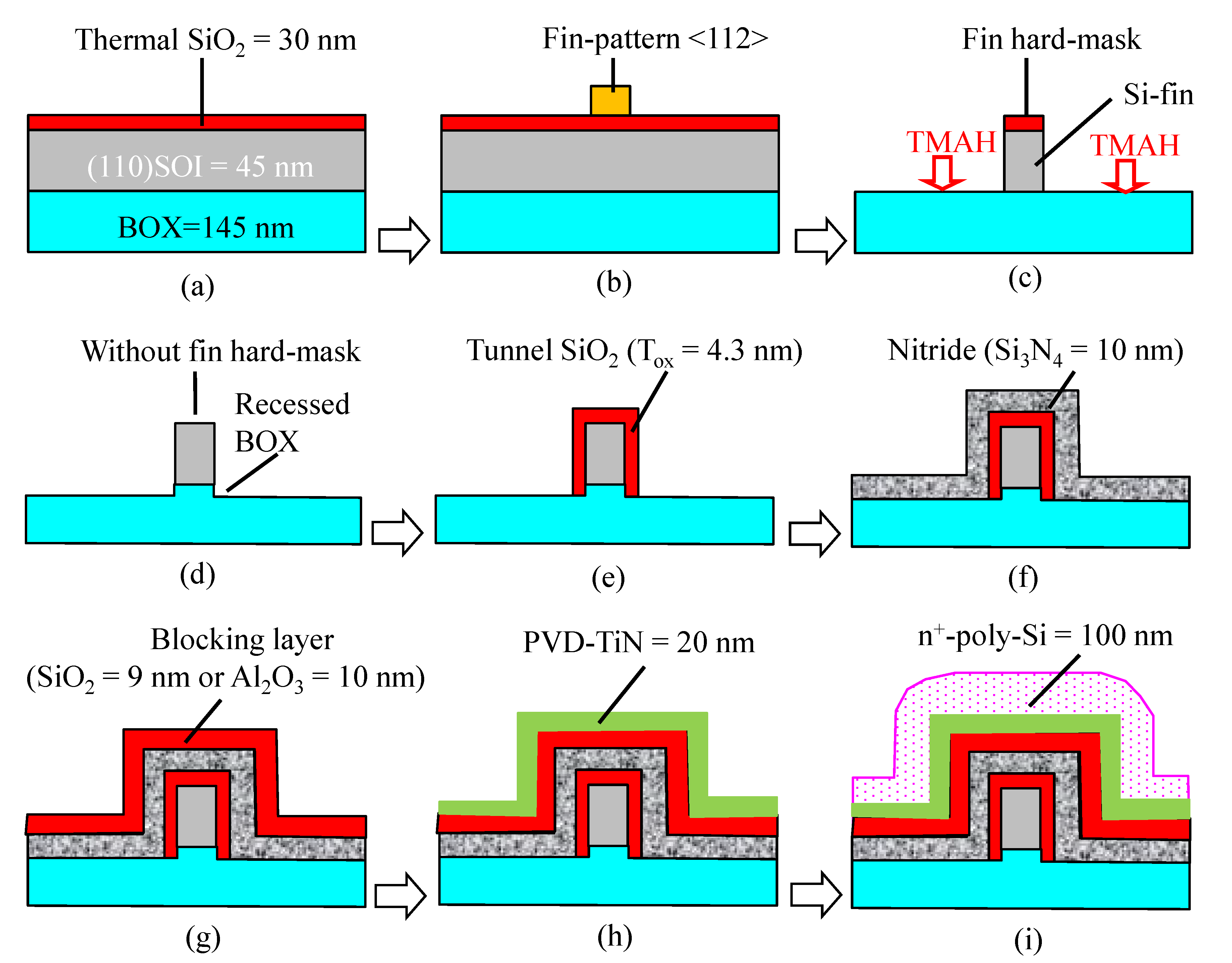
The schematic device fabrication process flow for the CT type SOI-FinFET flash memory is shown in
Figure 2. First, the lightly doped p-type (110)-SOI wafers were thermally oxidized to form a 30-nm-thick SiO
2 layer as shown in
Figure 2a, and fin-patterns were delineated in parallel to the <112> direction by using electron-beam (EB) lithography as shown in
Figure 2b. The trimming of EB-resist was performed using oxygen plasma to reduce the fin width. The fin-patterns were then transferred to the SiO
2 layer on the (110)-SOI wafers by reactive ion etching (RIE). After removing the EB-resist, further narrowing of the width of SiO
2 hard-mask was carried out with dilute hydrofluoric acid (DHF) solution. By using these techniques, the width of SiO
2 hard-mask was controlled to around 20 nm.
Figure 2.
Schematic device fabrication process flow for the CT type SOI-FinFET flash memory. (a) Thermal oxidation; (b) fin-pattern formation by electron-beam (EB) lithography; (c) fin-channel formation by the orientation-dependent wet etching; (d) SiO2 hard-mask removing by RIE; (e) tunnel oxide (Tox) formation by thermal oxidation; (f) nitride (Si3N4) layer deposition by LPCVD; (g) blocking layer (Al2O3 for MANOS and SiO2 for MONOS) deposition; (h) PVD-TiN deposition; (i) n+-poly-Si deposition.
Through the SiO
2 hard-masks, fin-channels were fabricated by the orientation-dependent wet etching with a 2.38% tetramethylammonium hydroxide (TMAH) solution at 50 °C for 30 s, as shown in
Figure 2c. Since the sidewalls of the fin-channels have a (111)-oriented plane with an extremely low etching rate in TMAH compared with other planes, very narrow and straight fin-channels can easily be fabricated. It was experimentally confirmed that the etching rates for (100)-, (110)-, and (111)-oriented Si wafers were 214, 359, and 9 nm/min, respectively [
44]. This indicates that the (111) plane is successfully retained in the etching process. To fabricate TG structure, the SiO
2 hard-mask layer was removed by RIE as show in
Figure 2d, which results in a slight reduction of fin-height. A recessed BOX region was also formed in this RIE process, which is useful for the suppression of SCE [
39,
40,
41].
After the fin-channel formation, a 4.3-nm-thick tunnel oxide (T
ox) layer was formed by thermal oxidation at 850 °C as shown in
Figure 2e, followed by the deposition of a 10-nm-thick Si
3N
4 layer as the charge trap** layer by low-pressure chemical vapor deposition (LPCVD) at 790 °C as shown in
Figure 2f. As the blocking layer, a 9-nm-thick tetraethylorthosilicate (TEOS)-SiO
2 layer was deposited for MONOS type devices by plasma CVD at 350 °C, and a 10-nm-thick Al
2O
3 layer was deposited for MANOS type device by atomic layer deposition (ALD) at 300 °C as shown in
Figure 2g. In the ALD deposition, we used trimetylaluminum (TMA) and water gas at pressure of 14 hPa. As the same gate material, a combination of a 20-nm-thick PVD-TiN layer and a 100-nm-thick n
+-poly-Si layer, was deposited on all wafers as shown in
Figure 2h,i. The gate electrodes were also patterned by EB lithography and fabricated by using combination of inductively coupled plasma (ICP) RIE for n
+-poly-Si and wet etching for PVD-TiN. In the PVD-TiN wet etching, we used an ammonium hydroxide (NH
4OH):hydrogen peroxide (H
2O
2):deionized water (H
2O) = 1:2:5 (APM) solution at 60 °C, which provides a high etching selectivity of PVD-TiN to SiO
2 [
45,
46].
After etching the top ONA and ONO layers on the fin extension and SD electrode regions by RIE, arsenic (As) ion implantation (I/I) was performed for SD-extension with a dose (
D) of 4 × 10
14 cm
−2 and a tilting angle (θ) of 60° at a fixed implant energy of 5 keV [
47]. Then, an 80-nm-thick gate sidewall spacer was formed by deposition of TEOS-SiO
2 and RIE. For the SD-region I/I, phosphorus ion (P
+) was used with
D = 1.5 × 10
15 cm
−2 and θ = 7°, which was followed by the deposition of a 100-nm-thick TEOS-SiO
2 layer on all wafers. To activate the implanted impurities, rapid thermal annealing (RTA) was performed at 830 °C for 2 s. Finally, contact holes and aluminum electrodes were formed, and all wafers were sintered in forming gas ambient at 450 °C for 30 min.
3. Results and Discussion
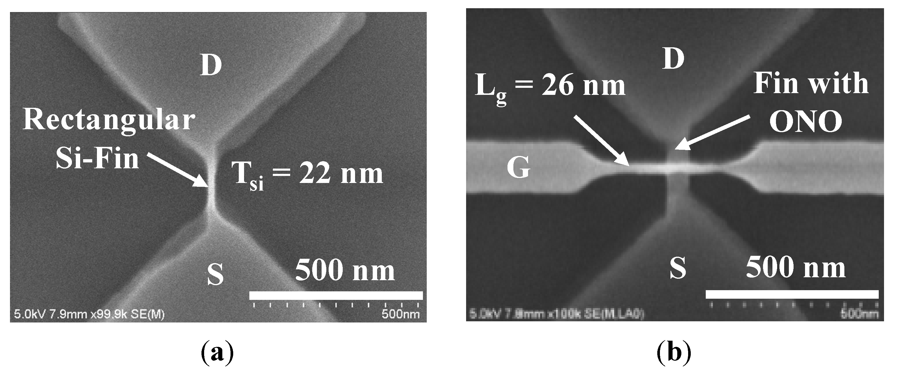
The scanning electron microscopy (SEM) images of the fabricated MANOS type SOI-FinFET flash memory after fin-channel formation and gate formation are shown in
Figure 3a,b, respectively. Note that a straight 22-nm-thick Si-fin channel is successfully fabricated thanks to the orientation-dependent wet etching. Moreover, a scaled 26-nm gate is also clearly confirmed.
Figure 3.
SEM images of the fabricated CT type SOI-FinFET flash memory (a) after fin-channel formation by the orientation-dependent wet etching and (b) after gate formation.
Figure 3.
SEM images of the fabricated CT type SOI-FinFET flash memory (a) after fin-channel formation by the orientation-dependent wet etching and (b) after gate formation.
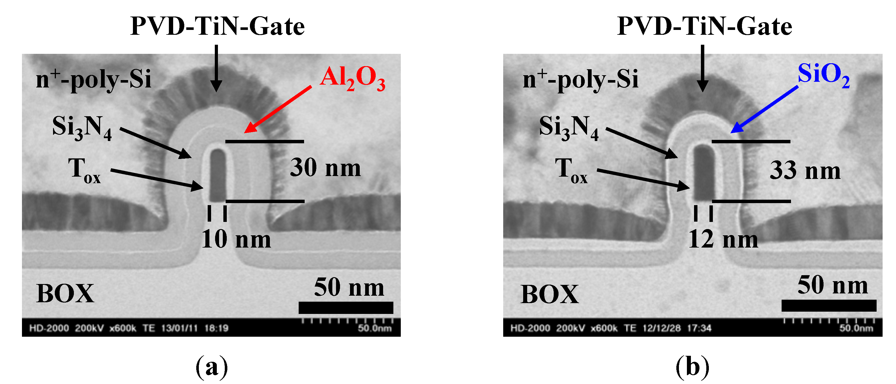
Figure 4a,b show the cross-sectional scanning transmission electron microscopy (STEM) images of the fabricated MANOS and MONOS type SOI-FinFET flash memories, respectively. Note that ultrathin and ideal rectangular cross-sectional Si fin-channels are fabricated uniformly. It should be mentioned that the fin-width and fin-height were slightly narrowed and lowered during wafer cleaning and tunnel oxide formation. Moreover, it is clearly confirmed that a uniform tunnel oxide layer is formed on top and sidewalls of the fin-channels without a thick SiO
2 hard-mask on top of Si fin-channel. This indicates that TG structure is fabricated successfully. Furthermore, it can be seen from STEM images that the charge trap** ONA and ONO layers are not only formed around the top and sidewalls of the fin-channels but also extended to the recessed BOX region. Such a gate all around (GAA) like structure is useful to the suppression of SCE as mentioned before. The observed a thin SiO
2 blocking layer (<9 nm) in
Figure 4b probably depends on the pick-up position of STEM sample owing to the poor uniformity of TEOS-SiO
2 layer thickness on a wafer although a 9-nm-thick TEOS-SiO
2 layer was confirmed on a dummy wafer as mentioned before.
Figure 4.
Cross-sectional STEM images of the fabricated (a) MANOS type SOI-FinFET flash memory with an Al2O3 blocking layer; and (b) MONOS type SOI-FinFET flash memory with a SiO2 blocking layer.
Figure 4.
Cross-sectional STEM images of the fabricated (a) MANOS type SOI-FinFET flash memory with an Al2O3 blocking layer; and (b) MONOS type SOI-FinFET flash memory with a SiO2 blocking layer.
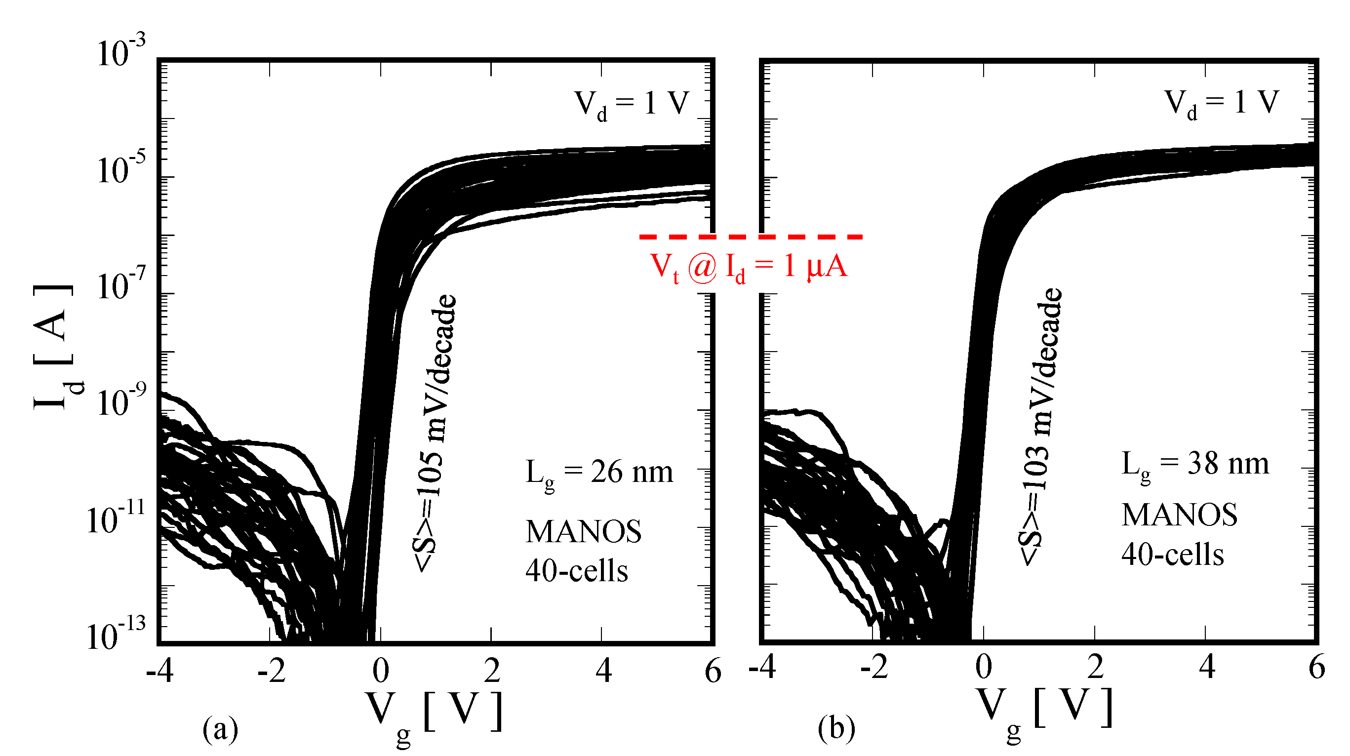
At first, we evaluated the V
t variability and SCE immunity for the fabricated MANOS and MONOS type SOI-FinFET flash memories with different gate length (L
g) values from 26 to 103 nm.
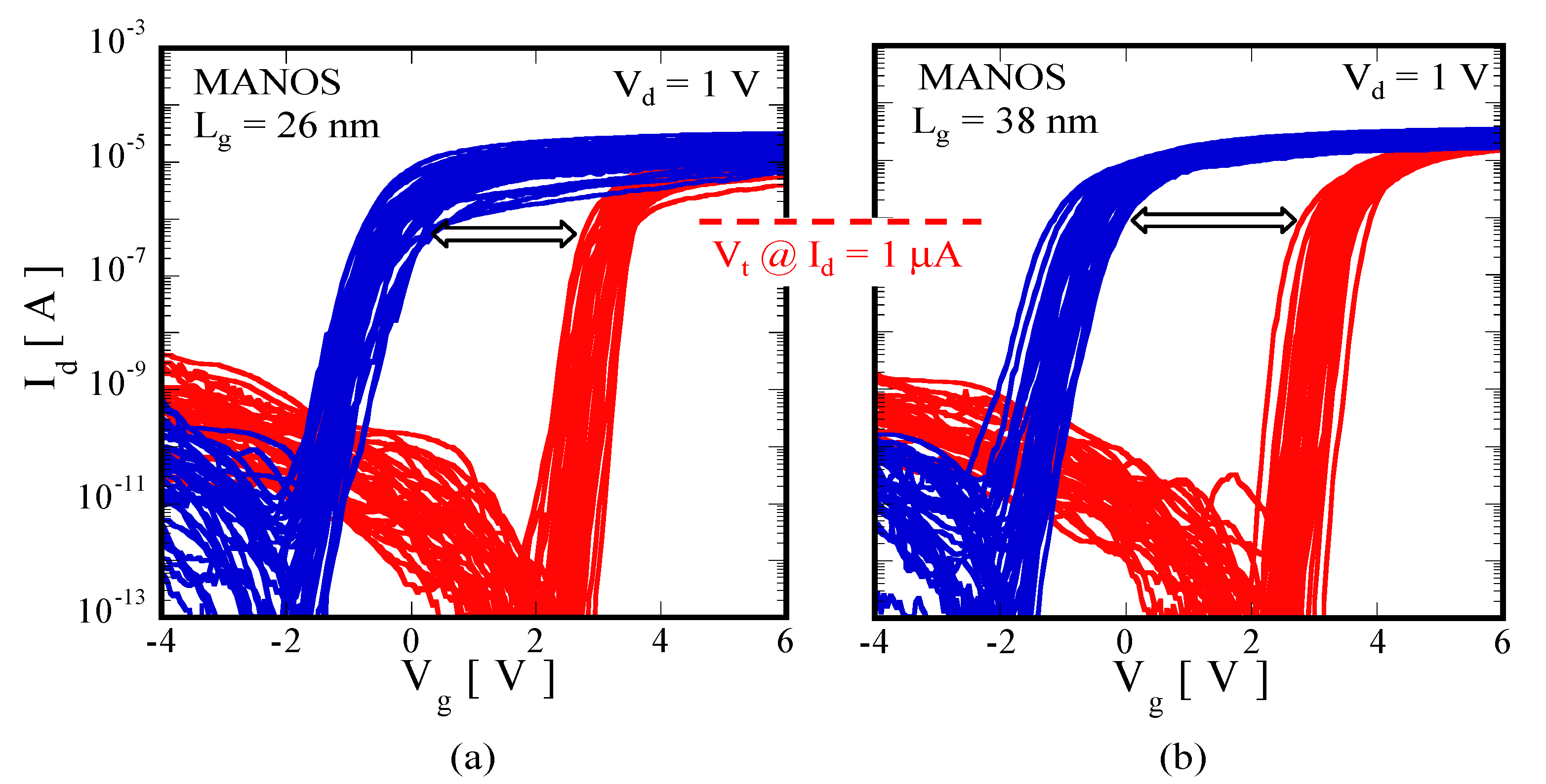
Figure 5a,b show the measured initial I
d-V
g characteristics of the fabricated MANOS type flash memories with different L
g values of 26 and 38 nm, respectively. In this measurement, we used 40 cell transistors for each type to investigate statistical V
t variations. Note that an excellent S-slope of 105-mV/decade is obtained even L
g is scaled down to 26 nm due to the GAA like structure. However, the uniformity of I
d-V
g curve is slightly deteriorated with scaling down L
g from 38 to 26 nm.
To evaluate V
t variations quantitatively, we measured the initial V
t values at a constant drain current of I
d = 1 μA for all devices with different L
g values from 26 to 103 nm.
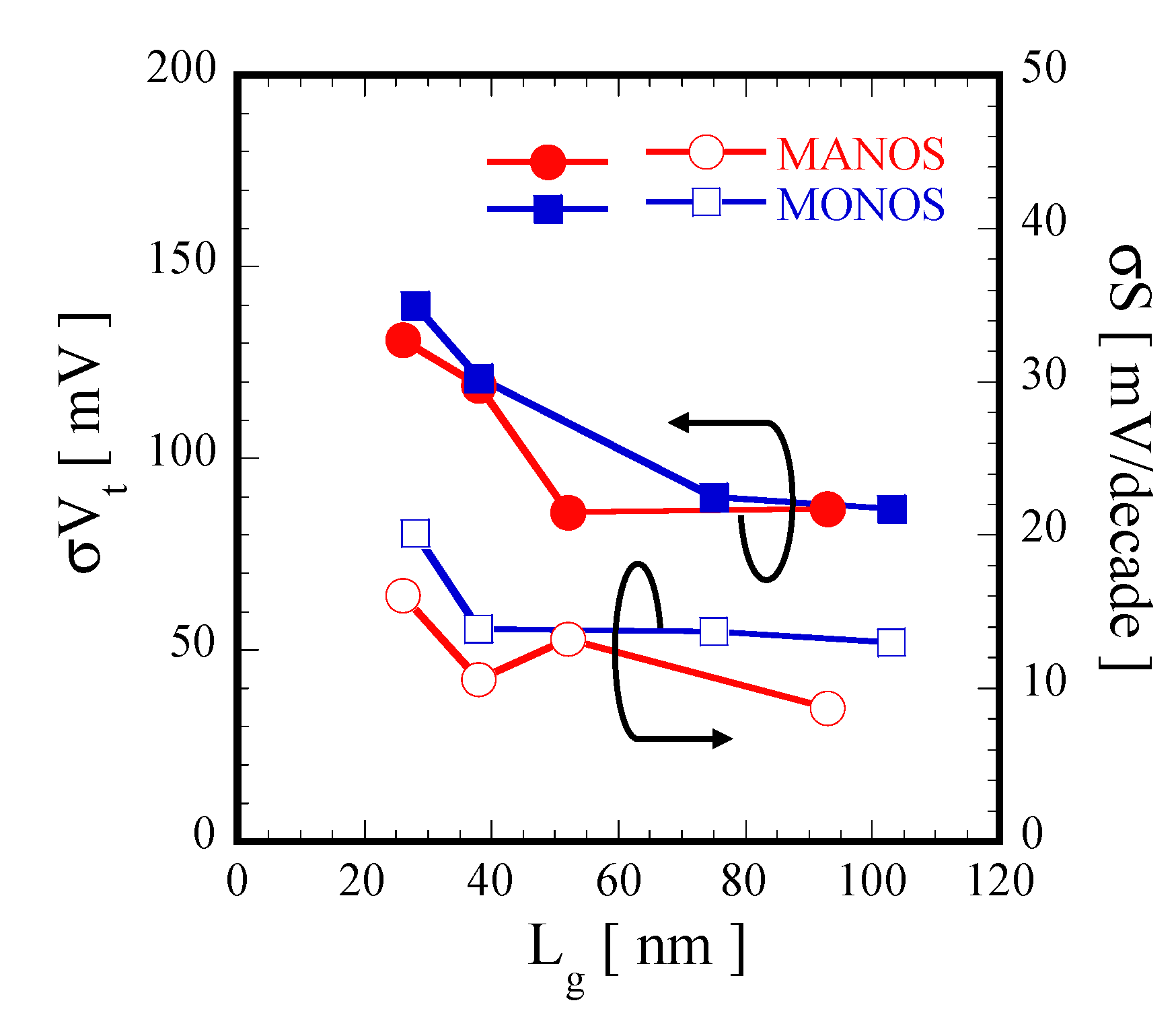
Figure 6 shows the measured standard deviations of V
t (σV
t) and S-slope (σS) as a function of L
g for the fabricated MANOS and MONOS type SOI-FinFET flash memories. It is clear that almost the same σV
t and σS are obtained for both types of devices although they increase slightly with scaling down L
g. This result indicates that the variations of V
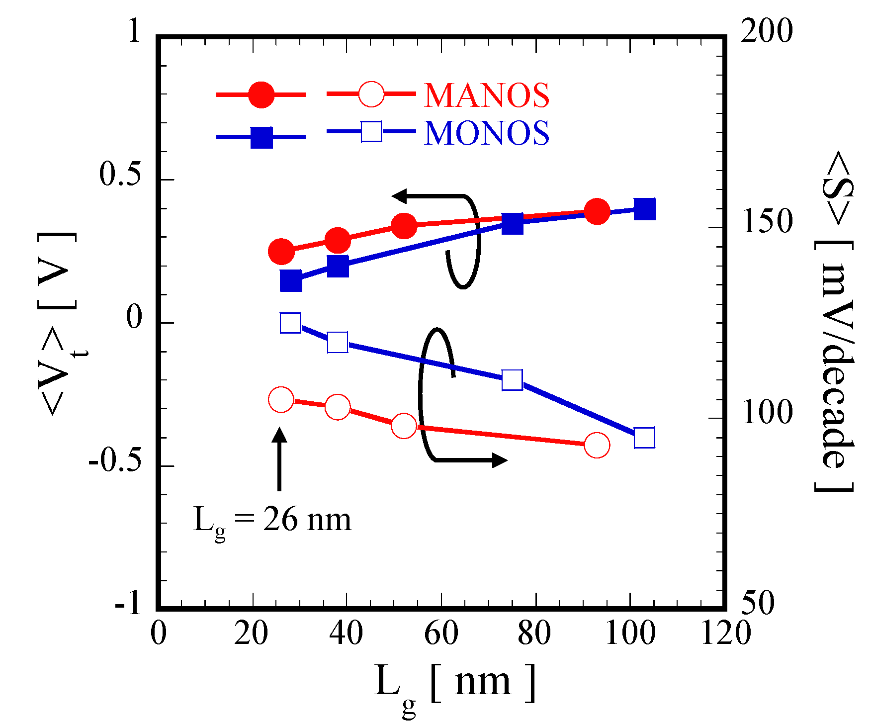
t and S-slope are almost independent of the blocking layer materials. The measured average V
t (<V
t>) and S-slope (<S>) values are summarized as a function of L
g as shown in
Figure 7. Note that the smaller V
t roll-off and the better S-slope are obtained in the MANOS devices than the MONOS ones at whole range of L
g due to the high-k effect of Al
2O
3 in MANOS type devices.
Figure 5.
Initial Id-Vg characteristics of the fabricated MANOS type SOI-FinFET flash memories with different Lg values of (a) Lg = 26 nm and (b) Lg = 38 nm.
Figure 5.
Initial Id-Vg characteristics of the fabricated MANOS type SOI-FinFET flash memories with different Lg values of (a) Lg = 26 nm and (b) Lg = 38 nm.
Figure 6.
σVt and σS as a function of Lg for the fabricated MANOS and MONOS type SOI-FinFET flash memories.
Figure 6.
σVt and σS as a function of Lg for the fabricated MANOS and MONOS type SOI-FinFET flash memories.
Figure 7.
Average Vt (<Vt>) and S-slope (<S>) values as a function of Lg for the fabricated MANOS and MONOS type SOI-FinFET flash memories.
Figure 7.
Average Vt (<Vt>) and S-slope (<S>) values as a function of Lg for the fabricated MANOS and MONOS type SOI-FinFET flash memories.
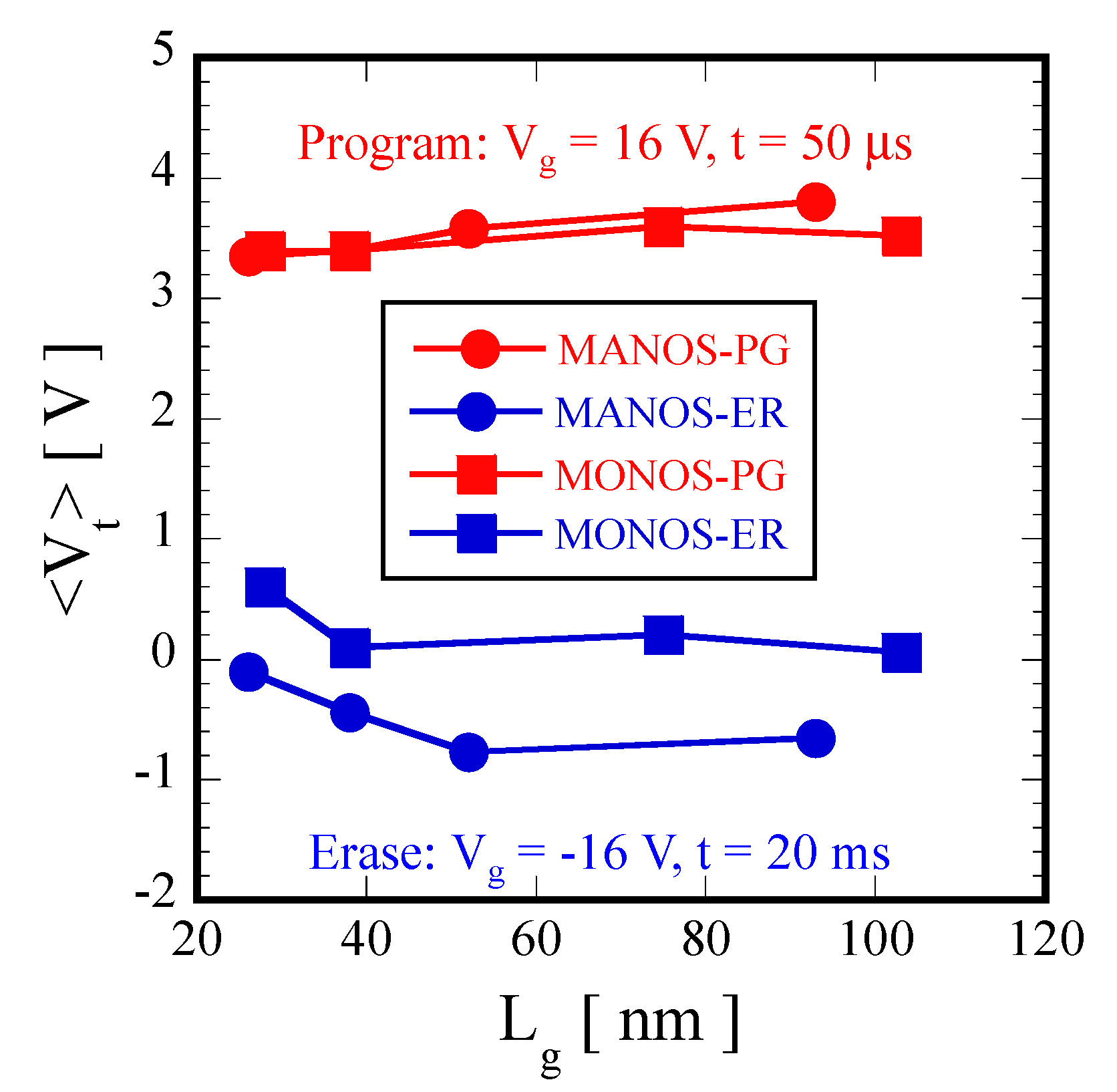
Before evaluation of memory characteristics, gate breakdown voltage was measured for the fabricated MANOS and MONOS type SOI-FinFET flash memory cell transistors. It was found that the gate breakdown voltage is around 17 V. According to this experimental result, P/E bias conditions were determined as V
g = 16 V, pulse-time (t) = 50 μs for programming, V
g = −16 V, t = 20 ms for erasing. In order to evaluate the dependence of the memory characteristics on the blocking layer materials, including V
t variability and memory window, the I
d-V
g characteristics of the fabricated MANOS and MONOS type devices with different L
g values were systematically investigated after one P/E cycle.
Figure 8a,b show the measured I
d-V
g characteristics of the fabricated MANOS type flash memory cell transistors with different L
g values of 26 and 38 nm after one P/E cycle, respectively. In this measurement, we used 40 cell transistors for each type. It is clear that a larger memory window is reasonably obtained in the long channel devices as compared to the short channel devices. A similar behavior was also observed in the MONOS type devices.
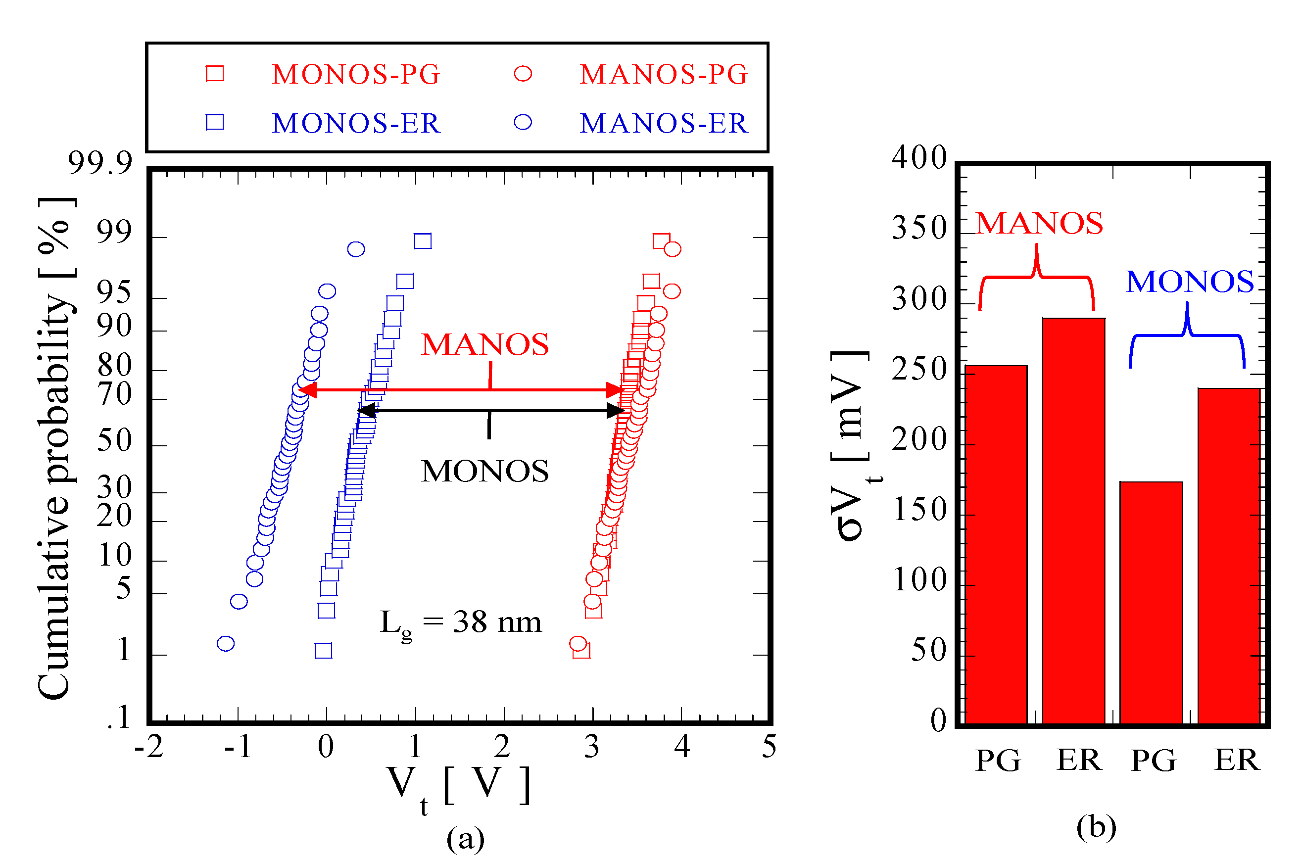
To compare the V
t variations between MANOS and MONOS type devices, V
t values for all fabricated devices were also evaluated at a constant drain current of I
d = 1 μA. As an example,
Figure 9 shows the measured cumulative probability of V
t and σV
t values for the MANOS and MONOS type devices with the same L
g of 38 nm after one P/E cycle. Note that a larger memory window is obtained in the MANOS type devices than the MONOS type ones due to the high-k effect of Al
2O
3 blocking layer in MANOS type devices. However, it is clear that σV
t values for both devices are almost the same although slightly smaller σV
t values are observed in the MONOS type device than MANOS type one. Such comparison was also carried out for all fabricated MANOS and MONOS type devices with different L
g values, and it was confirmed that actually a larger memory window is obtained in the MANOS type devices than the MONOS type ones at whole range of L
g as shown in
Figure 10. The deep erase in MANOS type devices should be resulted from the high-k effect of an Al
2O
3 (k ~ 9) blocking layer, which is efficient to enhance the electric field across the tunnel oxide and to reduce the electric field across the layer its self. Therefore, the electron back tunneling is effectively suppressed during erase operation which contributes to the deep erase in MANOS type devices [
28,
34].
Figure 8.
Id-Vg characteristics of the fabricated MANOS type SOI-FinFET flash memory cell transistors (40 cells) with different Lg values of (a) Lg = 26 nm and (b) Lg = 38 nm. P/E conditions: Vg = 16 V, t = 50 μs for program, and Vg = −16 V, t = 20 ms for erase.
Figure 8.
Id-Vg characteristics of the fabricated MANOS type SOI-FinFET flash memory cell transistors (40 cells) with different Lg values of (a) Lg = 26 nm and (b) Lg = 38 nm. P/E conditions: Vg = 16 V, t = 50 μs for program, and Vg = −16 V, t = 20 ms for erase.
Figure 9.
(a) Cumulative probability of Vt and (b) σVt of the fabricated MANOS and MONOS type SOI-FinFET flash memories with the same Lg of 38 nm after one P/E cycle. P/E conditions: Vg = 16 V, t = 50 μs for program, and Vg = −16 V, t = 20 ms for erase.
Figure 9.
(a) Cumulative probability of Vt and (b) σVt of the fabricated MANOS and MONOS type SOI-FinFET flash memories with the same Lg of 38 nm after one P/E cycle. P/E conditions: Vg = 16 V, t = 50 μs for program, and Vg = −16 V, t = 20 ms for erase.
Figure 10.
Average Vt (<Vt>) values as a function of Lg for the fabricated MANOS and MONOS type SOI-FinFET flash memory cell transistors after one P/E cycle. P/E conditions: Vg = 16 V, t = 50 μs for program, and Vg = −16 V, t = 20 ms for erase.
Figure 10.
Average Vt (<Vt>) values as a function of Lg for the fabricated MANOS and MONOS type SOI-FinFET flash memory cell transistors after one P/E cycle. P/E conditions: Vg = 16 V, t = 50 μs for program, and Vg = −16 V, t = 20 ms for erase.
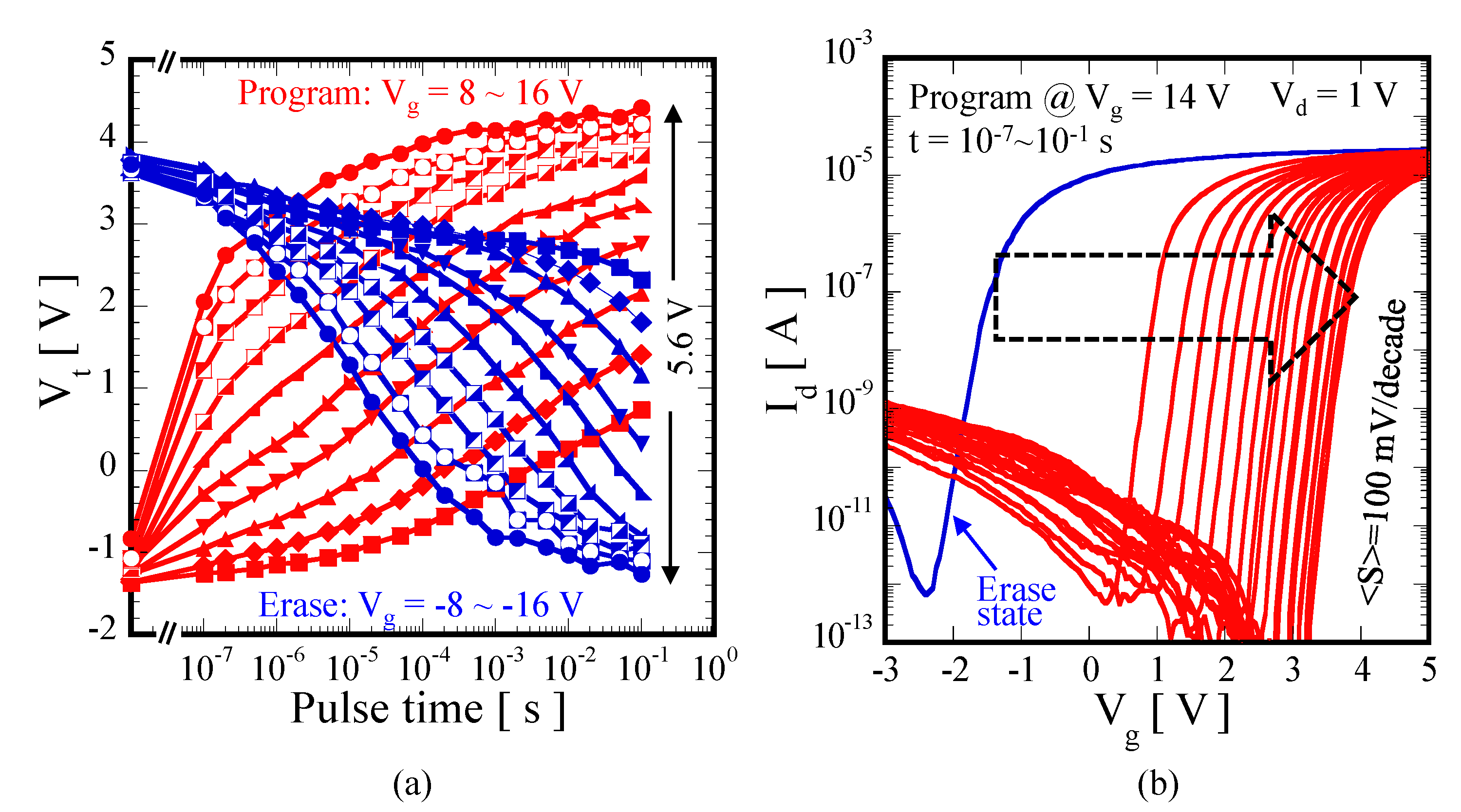
Figure 11a shows the measured P/E characteristics of the fabricated MANOS type device with L
g of 93 nm at different |V
g| values, and the program-time dependence of the I
d-V
g characteristics at V
g of 14 V is shown in
Figure 11b. It is clear that a large memory window of 5.6 V is obtained kee** an excellent S-slope of 100-mV/decade due to the GAA like structure.
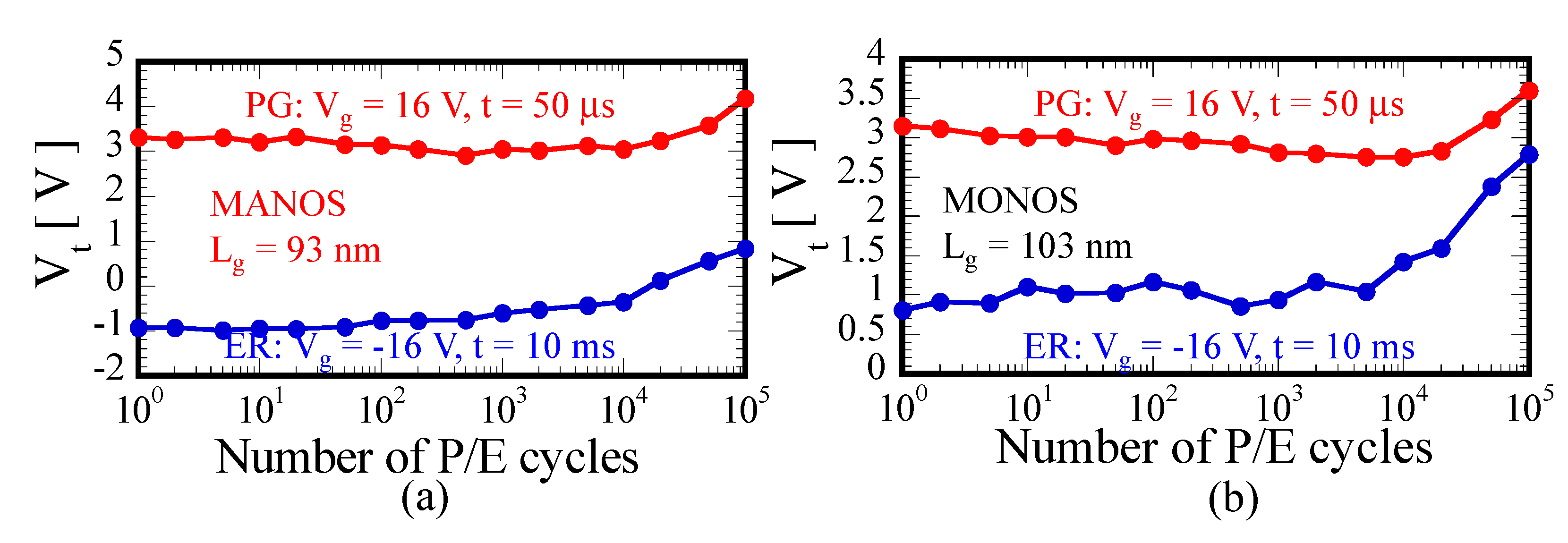
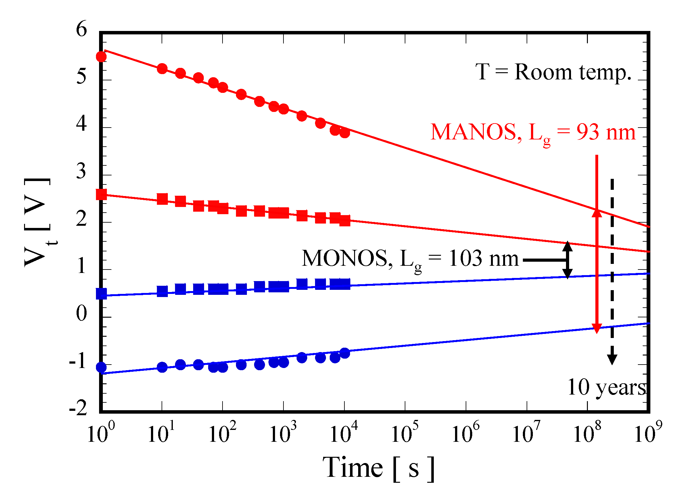
Figure 12a,b show the measured endurance characteristics of the fabricated MANOS and MONOS type devices, respectively. Note that these two kinds of device can operate over 100 k cycles although somewhat remarkable degradation is observed in the MONOS type device after 10 k cycles probably due to the insufficient uniformity of CVD-SiO
2 blocking layer. Moreover, the better data retention is obtained in the MANOS type device than MONOS type one due to the uniform ALD-Al
2O
3 blocking layer as shown in
Figure 13.
Figure 11.
(a) P/E characteristics and (b) program-time dependence of the Id-Vg characteristics of the fabricated MANOS type SOI-FinFET flash memory with Lg = 93 nm.
Figure 11.
(a) P/E characteristics and (b) program-time dependence of the Id-Vg characteristics of the fabricated MANOS type SOI-FinFET flash memory with Lg = 93 nm.
Figure 12.
Endurance characteristics of the fabricated (a) MANOS type SOI-FinFET flash memory with Lg = 93 nm; and (b) MONOS type SOI-FinFET flash memory with Lg = 103 nm.
Figure 12.
Endurance characteristics of the fabricated (a) MANOS type SOI-FinFET flash memory with Lg = 93 nm; and (b) MONOS type SOI-FinFET flash memory with Lg = 103 nm.
Figure 13.
Retention characteristics of the fabricated MANOS type SOI-FinFET flash memory with Lg = 93 nm and MONOS type SOI-FinFET flash memory with Lg = 103 nm at room temperature.
Figure 13.
Retention characteristics of the fabricated MANOS type SOI-FinFET flash memory with Lg = 93 nm and MONOS type SOI-FinFET flash memory with Lg = 103 nm at room temperature.


