Article

Design of a Wideband Doherty Power Amplifier with High Efficiency for 5G Application

1
Department of Electronics and Telecommunications, Politecnico di Torino, 10129 Turin, Italy
2
Department of Electronic, Faculty of Engineering, University of Zanjan, Zanjan 45371-38791, Iran
3
Microwave Engineering Center for Space Applications (MECSA), 00133 Rome, Italy
*
Author to whom correspondence should be addressed.
Electronics 2021, 10(8), 873; https://doi.org/10.3390/electronics10080873
Submission received: 8 March 2021 / Revised: 29 March 2021 / Accepted: 30 March 2021 / Published: 7 April 2021
(This article belongs to the Special Issue 5G Front-End Transceivers)

Abstract

:
This paper discusses the design of a wideband class AB-C Doherty power amplifier suitable for 5G applications. Theoretical analysis of the output matching network is presented, focusing on the impact of the non-ideally infinite output impedance of the auxiliary amplifier in back off, due to the device’s parasitic elements. By properly accounting for this effect, the designed output matching network was able to follow the desired impedance trajectories across the 2.8 GHz to 3.6 GHz range (fractional bandwidth = 25%), with a good trade-off between efficiency and bandwidth. The Doherty power amplifier was designed with two 10 W packaged GaN HEMTs. The measurement results showed that it provided 43 dBm to 44.2 dBm saturated output power and 8 dB to 13.5 dB linear power gain over the entire band. The achieved drain efficiency was between 62% and 76.5% at saturation and between 44% and 56% at 6 dB of output power back-off.

1. Introduction

Recently, with the continuous evolution of wireless systems towards higher data rates and lower power consumption, the need for high-performance transceivers has increased [1,2,3]. Independent of the specific scenario (base-station, handset, point-to-point radio-links), the power amplifier is one of the most consuming elements of the entire architecture, and it is of paramount importance for it to achieve the highest possible efficiency. This holds true for 5G systems, where PAs are required to provide high efficiency, gain, linearity, and output power in increasingly wider bandwidths [4,5,6,7]. The frequency bands for 5G mobile networks are organized into two different ranges, namely FR1 covering the sub-6 GHz bands, some of which were already used by previous standards, and FR2 covering the millimeter wave range, from 24.25 GHz to 52.6 GHz. To achieve high data rates, Orthogonal Frequency Division Modulation (OFDM) schemes are used in modern mobile communications systems, including 5G [8,9]. However, while the wider RF bandwidths achievable in the FR2 range allow relaxing the complexity of the adopted modulation schemes, PAs working in the FR1 range need to operate as efficiently as possible with modulations as complex as 4096-Quadrature Amplitude Modulation (QAM). These kinds of modulations feature a time-varying envelope with a very high peak-to-average power ratio (PAPR); therefore, to cope with such signals, power amplifiers are required to have high efficiency, not only at saturation, but also at lower output power levels [10,11,12,13]. This is not the case for conventional power amplifiers, which can have very high efficiency at their maximum output power, but show a sharp efficiency drop with output power back-off [14]. In order to increase back-off efficiency, various techniques have been proposed, both at the PA and at the system level, such as the Doherty power amplifier [13,15] and the Chireix outphasing [16,17] PA, based on the load modulation concept [18], or Envelope Elimination and Restoration (EER) [19,20] and Envelope Tracking (ET) [21,22] techniques, based instead on supply modulation. A combination of both supply and load modulation can be also exploited to maximize the achievable back-off efficiency [23,24]. Among all these techniques, however, the Doherty Power Amplifier (DPA) gained the highest popularity thanks to its architecture simplicity and relatively good linearity [25,26]. However, one of the main open issues of DPAs is related to bandwidth [27,28]. Although various techniques have been reported to increase the bandwidth of Doherty power amplifiers [29,30,31,32,33], they typically have the drawback of increasing the circuit complexity of the DPA. For instance, in [9,12], output compensation stages and post matching networks were added to improve bandwidth, while Reference [3] adopted a non-conventional impedance inverting network. Finally, digital techniques were used in [16,17]. Therefore, a Doherty power amplifier that can achieve a wide bandwidth and high efficiency by kee** its simple original topology is highly desirable [34].
This paper details the development of a wideband 20 W DPA with 6 dB Output power Back-Off (OBO) working in the frequency range from 2.8 GHz to 3.6 GHz, based on the CGH40010F GaN HEMT from Wolfspeed. The target frequency range was selected so as to cover as much as possible the 5G n78 band (3.3 GHz–3.8 GHz) within the limits of the selected device, which are mainly related to the package.
A main limitation to wideband DPA operation is due to the parasitic elements of the transistor. In particular, they make the output impedance of the auxiliary PA in back-off finite and also frequency dependent. This load variation was taken into account in the design of the main matching network, thus achieving wideband performance. The achieved Drain Efficiency (DE) at saturation and at 6 dB OBO was above 62% and 44%, respectively. The measured output power and power gain (at OBO) were, respectively, in excess of 43 dBm and 8 dB.
The paper is organized as follows. In Section 2, the overall structure of the proposed DPA is shown and the design of the output section is discussed. Section 3 and Section 4 present the simulated and measured performance, respectively, and compare this work with the literature. Finally, conclusions are drawn in Section 5.

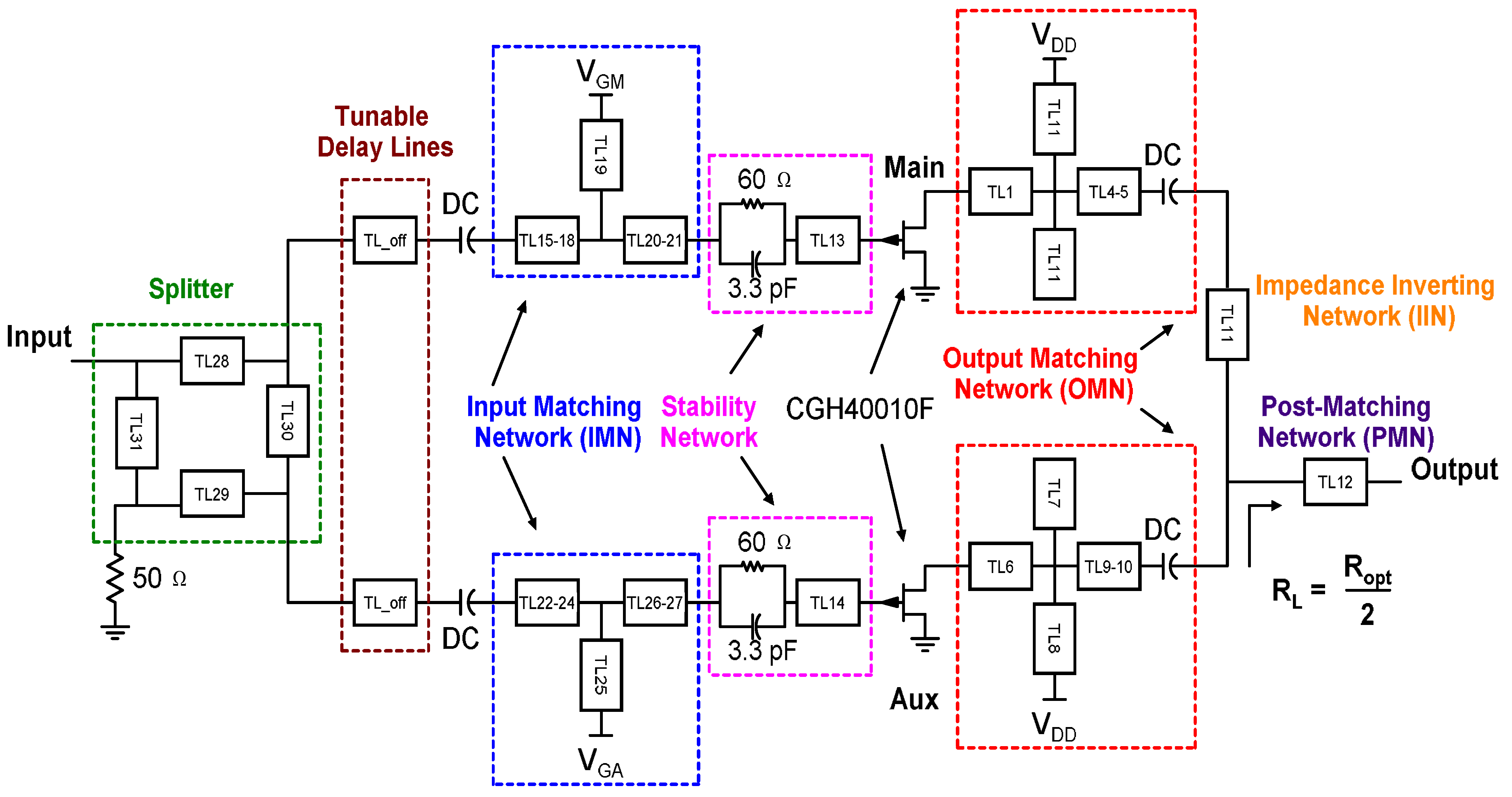
2. Doherty Power Amplifier Design

The schematic of the proposed DPA is illustrated in Figure 1, highlighting its building blocks. The DPA consists of main and auxiliary amplifiers, both based on the same active device biased in class AB and C, respectively. When the input power is low, the main amplifier is ON, and the auxiliary amplifier is OFF. Increasing the input power, the main amplifier reaches its maximum output voltage, and the first peak of efficiency occurs. At that point (break point), the auxiliary amplifier turns on and modulates the load of the main amplifier by injecting current at the common node. In this way, the output voltage and efficiency of the main amplifier remain, in principle, at the maximum value, while the output current and hence output power increase. The theoretical drain efficiency of the DPA is given by:
η D = P out P DC = 100 0.5 V out I out V DC,M I DC,M + V DC,A I DC,A
where V out and I out are the maximum RF output voltage and current at the fundamental frequency, while V DC,M I DC,M and V DC,A I DC,A are the DC power of the main and auxiliary PA, respectively. The output power back-off of the DPA is defined as:
O B O = 10 log 10 P out,B P out,S
where P out,B and P out,S are the output power levels at the break and saturation points, respectively. Theoretically, the drain efficiency at the break point is equal to the efficiency at saturation and remains high in the entire Doherty region (6 dB in this case). However, because of the parasitic components of the transistors and the knee voltage effect that causes soft auxiliary turn-on, the efficiency profile shows a drop in the Doherty region, and the practically attainable efficiency at the break point is typically lower than the saturated one [35,36].

2.1. Device Analysis

The CGH40010F GaN HEMT from Wolfspeed (Wolfspeed, Durham, NC, USA) was adopted to design the DPA. The Maximum Available Gain (MAG) of this device for different bias voltages is shown in Figure 2. As shown in Figure 3, the maximum frequency (around 26 GHz) and cut-off frequency (around 11.3 GHz) are only slightly dependent on the bias voltages, V GS and V DS ; thus, they do not represent a limit for the bias selection. The drain voltage was set to 28 V, which was compatible with the maximum frequency and voltage swing.
The maximum performance of the DPA in terms of output power and efficiency was achieved when the transistor was matched to its optimum intrinsic resistance. Hence, it was necessary to account for the parasitic effects of the transistor. For this reason, load-pull analysis at the extrinsic device reference plane over the whole bandwidth was used to find the actual optimum impedance. As an example, the simulated load-pull contours for the drain efficiency (blue) and the output power (red) at 3.3 GHz are reported in Figure 4a. Through load-pull analysis across the whole bandwidth, the optimum output load trajectories for the main and auxiliary transistors were found from 2.8 GHz to 3.6 GHz, both at saturation and the break point, as reported in Figure 4b. As a first step for designing the output matching networks, the average output impedance was considered, which was estimated in (17 + j5) Ω and (12 + j14) Ω at saturation and the break point, respectively. Then, wideband Computer-Aided Design (CAD) optimization was performed on the designed Output Matching Networks (OMNs) to fine-tune their behavior across the bandwidth.

2.2. Output Matching Network Design

According to the notation in Figure 5a, the input reflection coefficient ( Γ M ) of the main OMN is defined as [35]:
Γ M = S 11 + S 12 S 21 Γ M1 1 S 22 Γ M1
where the scattering parameters are defined with respect to R opt , and the load reflection coefficient of the OMN ( Γ M1 ) is expressed as:
Γ M1 = Z M1 R opt Z M1 + R opt
where Z M1 is the load impedance of the main OMN. R opt is the intrinsic resistance that simultaneously maximizes drain voltage and current, Z M1 , for an ideal DPA is defined as follows:
Z M1 = R opt ( 2 β )
where β is the ratio between the auxiliary and main current ( β = I A / I M ). Since in this design, a symmetrical structure was used, the theoretical maximum current for the main and auxiliary was the same. As a result, β was equal to zero and one at the break point and saturation, respectively ( Z M1 equal to 2 R opt and R opt ).
The output matching network needs to match the optimum output impedance found from the load-pull analysis with Z M1 . The common load R L was set to R opt / 2 and transformed into Z M1 by the Impedance Inverting Network (IIN), which is typically implemented with a quarter-wave ( λ /4) line. The electrical length of the λ /4 line changes with the frequency as follows:
θ = π 2 f f 0
where f is the operating frequency and f 0 is the center frequency at which the line was designed. Moreover, due to the parasitic elements of the transistors, the impedance presented by the auxiliary when in the OFF state was not infinite, but can be expressed as:
Z Aux = R Aux + j X Aux
To analyze the impact of Z Aux on the DPA behavior, the transformed impedance of the IIN is rewritten as follows [35]:
Z M1 = Z 0 ( R L | | Z Aux ) + j Z 0 tan ( θ ) Z 0 + j ( R L | | Z Aux ) tan ( θ )
where Z 0 is the characteristic impedance of the IIN:
Z 0 = 2 R opt R L
By substituting Equations (6), (7) and (9) in (8), Z M1 at the break point ( Z M1 B ) is calculated as:
Z M1 B = R opt R opt X Aux tan π 2 f f 0 + j R L X Aux + R opt tan π 2 f f 0 R L R opt X Aux tan π 2 f f 0 + j R opt X Aux
where only the imaginary part of Z Aux is considered for simplicity. This amounts to assuming that the impedance presented by the auxiliary may not be an ideal open circuit due to partial parasitic compensation, but its resistive component is however negligible. Figure 5b illustrates the Z M 1 B at the break point for different frequencies when varying X Aux from 40 Ω to 500 Ω . To plot these graphs based on Equation (10), the R opt , R L , and f 0 were considered to be 50 Ω , 25 Ω , and 3.3 GHz, respectively. As demonstrated, the load impedance of main OMN at the OBO ( Z M 1 B ) varied sensibly with both the operating frequency and parasitic reactance of the auxiliary PA ( X Aux ), thus making the design of wideband DPAs challenging.
After considering the theoretical behavior mentioned above, the next step was the OMN design. The microstrip implementation on a Rogers RO4350B substrate (Rogers Corporation, Chandler, AZ, USA) ( ε r = 3.66; substrate height and metal thickness were 762 µm and 35 µm, respectively) was selected for this design. There are different strategies for designing a wideband matching network [35]. In this case, the stepped impedance technique was preferred. The final layout of the output matching network is presented in Figure 6a and includes the drain biasing network. According to the results obtained in Figure 5b, in the OMN design, the variation of load impedances in the OBO point was considered in order to maximize back-off efficiency. Figure 6b shows the input reflection coefficient ( S 11 ) presented by the main output matching network, which was computed with respect to 2 R opt , for different Z M 1 B values, corresponding to different frequencies and X Aux . This result confirmed that the designed OMN was able to follow the load impedance variations in back-off, achieving wideband matching. The same OMN was also adopted for the auxiliary device, since it was identical to the main one. This choice should also ensure a similar phase variation versus frequency in the two branches, thus easing the enforcement of the appropriate signal phase alignment, which is essential for the Doherty operation.

2.3. Input Matching Network Design

Once having set the OMN, the Input Matching Network (IMN) can be designed. The proper design of the IMN is crucial to maintain high efficiency and equalize gain over wide bandwidths. Source-pull analysis was therefore performed to find the optimum input impedances for the main and auxiliary, which were (considering again a mean value over the entire bandwidth) (5 + j30) Ω and (3.2 + j18.5) Ω , respectively, and were then matched to 50 Ω . The final layout of the input matching network is illustrated in Figure 7. As can be noted, also for the IMN, the stepped impedance approach was followed. The topology for both IMNs was the same; however, the values of the transmission lines were independently optimized to account for the different biasing class. A parallel RC network (R = 60 Ω and C = 3.3 pF) was inserted in series with the gate to ensure in-band stability with the lowest possible associated losses.
Finally, an uneven hybrid 90 (branch line) splitter was designed with a 50 Ω reference impedance at all ports to provide the necessary splitting of the input signal into the main and auxiliary paths with a 90 phase shift between them. The power splitting ratio was P Aux / P Main = 1.5 . Figure 8 shows the layout and the simulated behavior of the splitter. Return loss was below −10 dB over the entire band. The isolated port was connectorized to allow for the insertion of an external resistor with high power handling capabilities.

2.4. Stability Analysis

The DPA stability must be evaluated for the designed DPA to ensure its unconditional stability at all frequencies. The stability analysis with the Rollett approach is not entirely reliable for Doherty power amplifiers [37]. To investigate the stability of parallel multi-amplifier architectures, the technique proposed by Ohtomo [38] provides more reliable results.
According to the Ohtomo approach, the Nyquist method was applied, considering the number of clockwise rotations around the point 1 + j0 of the Nyquist plot of the open loop functions ( G iM , G oM , G iA , and G oA ), simulated adopting the setup shown in Figure 9, using ideal circulators at the gate and drain nodes. The Nyquist plots are shown in Figure 10 for frequency going from DC to 6 GHz. As shown, none of them enclosed the 1 + j0 point; therefore, the proposed DPA was stable.

3. Simulated DPA Performance

The simulated drain efficiency and gain versus output power over the target frequency range are presented in Figure 11. As shown, drain efficiency was above 44% over the 6 dB back-off region, and the maximum output power was approximately 44 dBm.
In addition, the linearity of the DPA was assessed in simulation. A two-tone analysis was first performed to evaluate the third and fifth Intermodulation Distortions (IMD3 and IMD5), which are plotted in Figure 12a as a function of input power. As shown, IMD3 and IMD5 were below −18 dBm and −34 dBm, respectively. To test instead the system-level behavior, the designed DPA was simulated under a modulated signal adopting a 16-QAM signal with a 5 MHz bandwidth and 6 dB PAPR. Figure 12b illustrates the simulated input and output power spectra at the center frequency of 3.3 GHz for an average output power of 36 dBm. As shown, the Adjacent Channel Power Ratio (ACPR) was less than −32 dBc. which compares well with the state-of-the-art [9,31], at least in simulation.

4. Measurements Results

The photograph of the fabricated DPA is shown in Figure 13. For the DPA characterization, the gate voltages of the main and auxiliary amplifiers were set to − 2.8 V and −5.5 V, respectively, while the drain voltage was 28 V. The quiescent drain current was 68 mA.
The simulated and measured scattering parameters are reported in Figure 14. Despite a frequency shift towards lower frequencies, a small signal gain around 10 dB was maintained from 2.2 GHz to 3.6 GHz, which allowed fully covering the targeted frequency band. Moreover, input matching around 10 dB was achieved from 2.6 GHz to 3.6 GHz. The output matching results were better than 10 dB in the higher portion of the operating band, namely from 3 GHz to 3.8 GHz, while this slightly degraded at the lower end of the band. To account for the possible inaccuracy of the capacitor and resistor models and mounting/soldering process, we inserted tunable elements in the matching networks. During the measurements, we tuned the networks and the bias to achieve the widest possible bandwidth, thus changing the circuit from the nominal/simulated condition. This led to some mismatches between the simulation and measurements.
Continuous Wave (CW) large signal measurements showed a maximum output power at 3 dB gain compression between 43 dBm and 44.2 dBm. Figure 15 shows the measured gain and drain efficiency with respect to the output power. The large signal performance is summarized and compared to simulations in Figure 16, which shows that the agreement between the measurements and simulations was rather good. The measured drain efficiency ranged from 62% to 76.5% at saturation and from 44% to 56% at 6 dB output power back-off. The obtained gain at 6 dB back-off over the frequency band was between 8 dB and 13.5 dB.
Table 1 summarizes the performance of the proposed DPA compared to other works where DPAs were designed targeting a similar OBO level on a comparable frequency range and adopting the same device. As discussed, in the proposed DPA, a high drain efficiency together with a high gain were achieved over a fairly wide bandwidth. The performance obtained was well in line with the state-of-the-art in this frequency range, demonstrating that the proposed simple, but effective wideband approach was suitable for 5G applications in the S-band.

5. Conclusions

A wideband class AB-C Doherty power amplifier using a 10W GaN HEMT device was presented. By considering the parasitic elements of the transistors and the variations of the transformed impedance at the back-off point, appropriate matching networks were designed to achieve wideband operation from 2.8 GHz to 3.6 GHz. The experimental results showed that an output power above 43 dB was reached together with a drain efficiency in excess of 62% and 44% at saturation and at 6 dB back-off, respectively. The results achieved in this first design were in line with the state-of-the-art. A re-design is on-going pushing toward 4 GHz, in order to better fit the 5G bandwidth. Harmonic tuning strategies are also being considered to further enhance the efficiency-bandwidth trade-off.

Author Contributions

Formal analysis, A.N. and M.E.; methodology, A.N., M.E. and S.T.; resources, A.N., M.E., S.T. and A.P.; supervision, S.T., M.P., V.C. and C.R.; validation, S.T. and A.P.; writing—original draft, A.N. and M.E.; writing—review and editing, S.T., A.P., M.P., V.C. and C.R. All authors have read and agreed to the published version of the manuscript.

Funding

This research received no external funding.

Data Availability Statement

The data presented in this study are available on request from the corresponding author.

Conflicts of Interest

The authors declare no conflict of interest.

References

  1. Chang, G.K.; Cheng, L.; Xu, M.; Guidotti, D. Integrated fiber-wireless access architecture for mobile backhaul and fronthaul in 5G wireless data networks. In Proceedings of the 2014 IEEE Avionics, Fiber-Optics and Photonics Technology Conference (AVFOP); IEEE: New York, NY, USA, 2014; pp. 49–50. [Google Scholar]
  2. Kang, H.; Lee, H.; Lee, W.; Oh, H.; Lim, W.; Koo, H.; Park, C.S.; Hwang, K.C.; Lee, K.Y.; Yang, Y. Octave bandwidth Doherty power amplifier using multiple resonance circuit for the peaking amplifier. IEEE Trans. Circuits Syst. Regul. Pap. 2018, 66, 583–593. [Google Scholar] [CrossRef]
  3. Li, C.; You, F.; Peng, J.; Wang, J.; Haider, M.F.; He, S. Co-Design of matching sub-networks to realize broadband symmetrical Doherty with configurable back-Off region. IEEE Trans. Circuits Syst. II Express Briefs 2019, 67, 1730–1734. [Google Scholar] [CrossRef]
  4. Abadi, M.N.A.; Golestaneh, H.; Sarbishaei, H.; Boumaiza, S. Doherty power amplifier with extended bandwidth and improved linearizability under carrier-aggregated signal stimuli. IEEE Microw. Wirel. Components Lett. 2016, 26, 358–360. [Google Scholar] [CrossRef]
  5. Estebsari, M.; Nasri, A.; Piacibello, A.; Ramella, C.; Camarchia, V.; Pirola, M. 3.1–3.6 GHz 22 W GaN Doherty power amplifier. In Proceedings of the 2020 23rd International Microwave and Radar Conference (MIKON); IEEE: New York, NY, USA, 2020; pp. 424–426. [Google Scholar]
  6. Nikandish, G.R.; Staszewski, R.B.; Zhu, A. Broadband fully integrated GaN power amplifier with minimum-inductance BPF matching and two-transistor AM-PM compensation. IEEE Trans. Circuits Syst. Regul. Pap. 2020, 67, 4211–4223. [Google Scholar] [CrossRef]
  7. Dehqan, A.; Toofan, S.; Medi, A. A highly efficient class-EF 2 power amplifier in GaAs pHEMT technology. Analog. Integr. Circuits Signal Process. 2017, 93, 197–203. [Google Scholar] [CrossRef]
  8. Muntean, V.H.; Otesteanu, M. WiMAX versus LTE—An overview of technical aspects for next generation networks technologies. In Proceedings of the 2010 9th International Symposium on Electronics and Telecommunications; IEEE: New York, NY, USA, 2010; pp. 225–228. [Google Scholar]
  9. Cheng, Z.; **ong, G.; Liu, Y.; Zhang, T.; Tian, J.; Guo, Y.J. High-efficiency Doherty power amplifier with wide OPBO range for base station systems. IET Microwaves Antennas Propag. 2019, 13, 926–929. [Google Scholar] [CrossRef]
  10. Pengelly, R.; Fager, C.; Ozen, M. Doherty’s legacy: A history of the Doherty power amplifier from 1936 to the present day. IEEE Microw. Mag. 2016, 17, 41–58. [Google Scholar] [CrossRef]
  11. Naah, G.; He, S.; Shi, W.; Li, C.; Nusenu, S.Y. Harmonic-tuned continuum mode active load modulation output combiner for the design of broadband asymmetric Doherty power amplifiers. IET Microwaves Antennas Propag. 2019, 13, 1226–1234. [Google Scholar] [CrossRef]
  12. Yu, C.; Su, Z.; Liu, Y.; Tang, B.; Li, S. Broadband filtering high-efficiency Doherty amplifier based on a novel post-matching network. In Proceedings of the 2019 European Microwave Conference in Central Europe (EuMCE); IEEE: New York, NY, USA, 2019; pp. 212–215. [Google Scholar]
  13. Rubio, J.M.; Fang, J.; Camarchia, V.; Quaglia, R.; Pirola, M.; Ghione, G. 3–3.6-GHz wideband GaN Doherty power amplifier exploiting output compensation stages. IEEE Trans. Microw. Theory Tech. 2012, 60, 2543–2548. [Google Scholar] [CrossRef]
  14. Dehqan, A.R.; Toofan, S.; Lotfi, H. Floating bulk cascode class-E power amplifier. IEEE Trans. Circuits Syst. II Express Briefs 2018, 66, 537–541. [Google Scholar] [CrossRef]
  15. Quaglia, R.; Camarchia, V.; Rubio, J.J.M.; Pirola, M.; Ghione, G. A 4-W Doherty power amplifier in GaN MMIC technology for 15-GHz applications. IEEE Microw. Wirel. Components Lett. 2017, 27, 365–367. [Google Scholar] [CrossRef] [Green Version]
  16. Piacibello, A.; Quaglia, R.; Pirola, M.; Cripps, S. Design of an S-Band chireix outphasing power amplifier based on a systematic bandwidth limitation analysis. In Proceedings of the 2018 13th European Microwave Integrated Circuits Conference (EuMIC); IEEE: New York, NY, USA, 2018; pp. 186–189. [Google Scholar]
  17. Cappello, T.; Florian, C.; Barton, T.W.; Litchfield, M.; Popovic, Z. Multi-level supply-modulated Chireix outphasing for LTE signals. In Proceedings of the 2017 IEEE MTT-S International Microwave Symposium (IMS); IEEE: New York, NY, USA, 2017; pp. 1846–1849. [Google Scholar]
  18. Ramella, C.; Piacibello, A.; Quaglia, R.; Camarchia, V.; Pirola, M. High efficiency power amplifiers for modern mobile communications: The load-modulation approach. Electronics 2017, 6, 96. [Google Scholar] [CrossRef] [Green Version]
  19. Bolotov, A.; Kholyukov, R.; Varlamov, O. EER power amplifier modulator efficiency improvement using PWM with additional sigma-delta modulation. In Proceedings of the 2018Systems of Signal Synchronization, Generating and Processing in Telecommunications (SYNCHROINFO); IEEE: New York, NY, USA, 2018; pp. 1–4. [Google Scholar]
  20. Vasić, M.; Garcia, O.; Oliver, J.A.; Alou, P.; Diaz, D.; Cobos, J.A.; Gimeno, A.; Pardo, J.M.; Benavente, C.; Ortega, F.J. Efficient and linear power amplifier based on envelope elimination and restoration. IEEE Trans. Power Electron. 2011, 27, 5–9. [Google Scholar] [CrossRef]
  21. **, Q.; Ruan, X.; Ren, X.; Wang, Y.; Leng, Y.; Chi, K.T. Series–parallel-form switch-linear hybrid envelope-tracking power supply to achieve high efficiency. IEEE Trans. Ind. Electron. 2016, 64, 244–252. [Google Scholar] [CrossRef]
  22. Alt, A.; Hirshy, H.; Jiang, S.; Lee, K.B.; Casbon, M.A.; Chen, P.; Houston, P.A.; Tasker, P.J.; Lees, J. Analysis of gain variation with changing supply voltages in GaN HEMTs for envelope tracking power amplifiers. IEEE Trans. Microw. Theory Tech. 2019, 67, 2495–2504. [Google Scholar] [CrossRef]
  23. Cappello, T.; Barton, T.W.; Florian, C.; Litchfield, M.; Popovic, Z. Multilevel supply-modulated Chireix outphasing with continuous input modulation. IEEE Trans. Microw. Theory Tech. 2017, 65, 5231–5243. [Google Scholar] [CrossRef]
  24. Fishler, D.; Popović, Z.; Barton, T. Supply modulation behavior of a Doherty power amplifier. IEEE J. Microwaves 2021, 1, 508–512. [Google Scholar] [CrossRef]
  25. Giofrè, R.; Colantonio, P.; Giannini, F.; Ramella, C.; Camarchia, V.; Iqbal, M.; Pirola, M.; Quaglia, R. A comprehensive comparison between GaN MMIC Doherty and combined class-AB power amplifiers for microwave radio links. Int. J. Microw. Wirel. Technol. 2016, 8, 673. [Google Scholar] [CrossRef]
  26. Camarchia, V.; Colantonio, P.; Giannini, F.; Giofrè, R.; Jiang, T.; Pirola, M.; Quaglia, R.; Ramella, C. A design strategy for AM/PM compensation in GaN Doherty power amplifiers. IEEE Access 2017, 5, 22244–22251. [Google Scholar] [CrossRef]
  27. Li, Y.; Fang, X.; Jundi, A.; Huang, H.; Boumaiza, S. Two-port network theory-based design method for broadband class J Doherty amplifiers. IEEE Access 2019, 7, 51028–51038. [Google Scholar] [CrossRef]
  28. Nasri, A.; Estebsari, M.; Toofan, S.; Piacibello, A.; Ramella, C.; Camarchia, V.; Pirola, M. A 3-3.8 GHz Class-J GaN HEMT power amplifier. In Proceedings of the 2020 23rd International Microwave and Radar Conference (MIKON); IEEE: New York, NY, USA, 2020; pp. 416–419. [Google Scholar]
  29. Kalyan, R.; Rawat, K.; Koul, S.K. Reconfigurable and concurrent dual-band Doherty power amplifier for multiband and multistandard applications. IEEE Trans. Microw. Theory Tech. 2016, 65, 198–208. [Google Scholar] [CrossRef]
  30. Barakat, A.; Thian, M.; Fusco, V.; Bulja, S.; Guan, L. Toward a more generalized Doherty power amplifier design for broadband operation. IEEE Trans. Microw. Theory Tech. 2016, 65, 846–859. [Google Scholar] [CrossRef] [Green Version]
  31. Sun, G.; Jansen, R.H. Broadband Doherty power amplifier via real frequency technique. IEEE Trans. Microw. Theory Tech. 2011, 60, 99–111. [Google Scholar] [CrossRef]
  32. Rubio, J.J.M.; Camarchia, V.; Pirola, M.; Quaglia, R. Design of an 87% fractional bandwidth Doherty power amplifier supported by a simplified bandwidth estimation method. IEEE Trans. Microw. Theory Tech. 2017, 66, 1319–1327. [Google Scholar] [CrossRef] [Green Version]
  33. Piacibello, A.; Quaglia, R.; Camarchia, V.; Ramella, C.; Pirola, M. Dual-input driving strategies for performance enhancement of a Doherty power amplifier. In Proceedings of the 2018 IEEE MTT-S International Wireless Symposium (IWS); IEEE: New York, NY, USA, 2018; pp. 1–4. [Google Scholar]
  34. Bathich, K.; Markos, A.Z.; Boeck, G. A wideband GaN Doherty amplifier with 35% fractional bandwidth. Eu. Microw. Conf. 2010, 1006–1009. [Google Scholar] [CrossRef]
  35. Pozar, D.M. Microwave Engineering; John Wiley & Sons: Hoboken, NJ, USA, 2011. [Google Scholar]
  36. Ghione, G.; Pirola, M. Microwave Electronics; Cambridge University Press: Cambridge, UK, 2017. [Google Scholar]
  37. Rollett, J. Stability and power-gain invariants of linear twoports. IRE Trans. Circuit Theory 1962, 9, 29–32. [Google Scholar] [CrossRef] [Green Version]
  38. Ohtomo, M. Stability analysis and numerical simulation of multidevice amplifiers. IEEE Trans. Microw. Theory Tech. 1993, 41, 983–991. [Google Scholar] [CrossRef]
Figure 1. Schematic of the proposed Doherty power amplifier.
Electronics 10 00873 g001
Figure 2. Simulated maximum available gain of the CGH40010F device for different biasing classes.
Electronics 10 00873 g002
Figure 3. Cut−off (a) and maximum (b) frequency of the CGH40010F versus V GS and V DS .
Electronics 10 00873 g003
Figure 4. (a) Load-pull contours for the drain efficiency (blue) and output power (red) at 3.3 GHz and (b) optimum output impedance at saturation and Output power Back-Off (OBO). DE, Drain Efficiency.
Electronics 10 00873 g004
Figure 5. (a) Block diagram of the output matching networks. (b) Variation of the Z M 1 B versus f (from 2.8 GHz to 3.6 GHz) and X Aux (from 40 Ω to 500 Ω ) when the auxiliary power amplifier (PA) is OFF.
Electronics 10 00873 g005
Figure 6. (a) Output matching network of the main (dimensions (width/length) are in mm) and (b) input reflection coefficient when port 1 is normalized with respect to 2 R opt for different load impedance at the break point.
Electronics 10 00873 g006
Figure 7. Layout of the input matching network (dimension: width/length (mm)).
Electronics 10 00873 g007
Figure 8. (a) Layout of the splitter (dimension: width/length (mm)). (b) Performance versus frequency.
Electronics 10 00873 g008
Figure 9. Implementation of the stability test on the Doherty power amplifier. IIN, Impedance Inverting Network.
Electronics 10 00873 g009
Figure 10. Nyquist plot of the open-loop function for the proposed Doherty power amplifier (DPA) from 100 MHz to 6 GHz.
Electronics 10 00873 g010
Figure 11. Simulated drain efficiency (a) and gain (b) of the designed DPA versus output power.
Electronics 10 00873 g011
Figure 12. (a) Two-tone power sweep simulation at 3.3 GHz. (b) Simulated input and output power spectrum at 3.3 GHz for the average output power of 36 dBm. IMD, Intermodulation Distortion.
Electronics 10 00873 g012
Figure 13. Photograph of the fabricated Doherty power amplifier.
Electronics 10 00873 g013
Figure 14. Simulated (dashed) and measured (solid) scattering parameters of the proposed DPA (a) S ( 2 , 1 ) , (b) S ( 1 , 1 ) , and (c) S ( 2 , 2 ) .
Electronics 10 00873 g014
Figure 15. Measured (a) drain efficiency and (b) gain versus output power.
Electronics 10 00873 g015
Figure 16. Comparison of simulated (solid) and measured (dashed) large signal performance versus frequency: (a) saturated output power and (b) drain efficiency and (c) gain at saturation and 6 dB back-off.
Electronics 10 00873 g016
Table 1. Comparison of this work with other designs based on the CGH40010F.
Ref.Freq.
(GHz)
Pout
(dBm)
DE Sat.
(%)
DE OBO
(%)
Gain
(dB)
[4]1.7–2.242.558–7248–558.2–10.2
[9]2.9–3.343.9–44.77040.6–44.26–11
[11]1.4–2.441.8–43.547.5–64.235.5–526–13
[12]2.2–2.643–4460–6545–536–10
[13]3–3.643–4455–6638–5612
[31]2.2–340.2–41.252–6830–536–10
[32]1.5–3.842.3–43.442–6333–5510–13.8
This Work2.8–3.643–44.262–76.544–568–13.5
Publisher’s Note: MDPI stays neutral with regard to jurisdictional claims in published maps and institutional affiliations.

