1. Introduction
This paper focuses on central processing units for real-time embedded systems (RTESs). The majority of microprocessors available on the market are not designed for hard RTESs [
1]. Advanced performance improvement techniques (pipelining, branch prediction units (BPUs), floating point units (FPUs), caching, memory management units (MMUs), frequency scaling, shared buses, etc.) sacrifice determinism and introduce
timing anomalies [
1,
2,
3] which increase the complexity of static timing analysis (STA) [
4,
5].
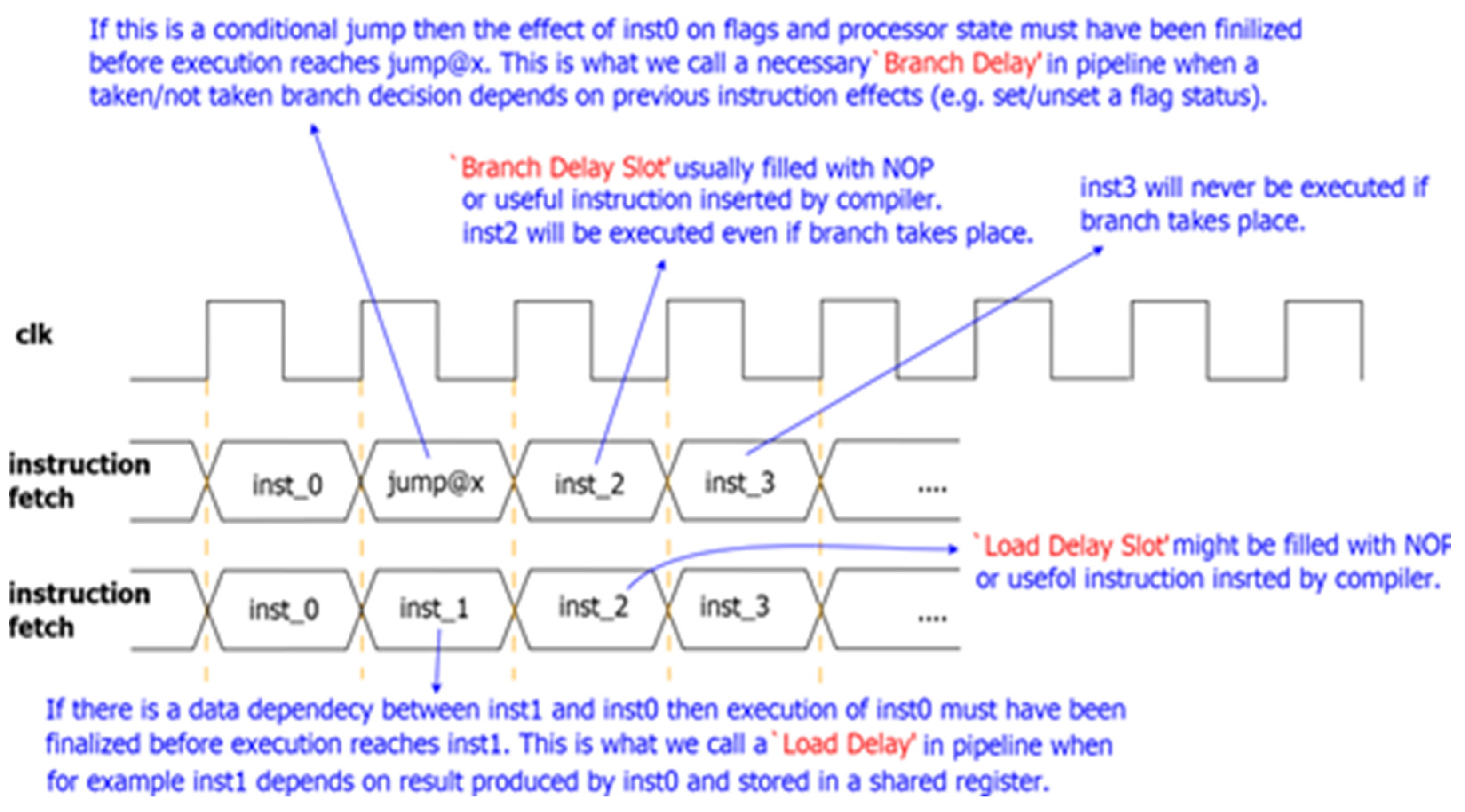
A good example of the increase in the complexity of STA is the case of a
pipeline stall, where execution of an instruction must stall (e.g., due to register data dependency) for
extra cycles where
depends on pipeline depth. Another example is incorrect predictions from the BPU, which forces the processor to discard speculatively fetched instructions, thus incurring a delay (equal to the number of stages between the fetch and execute stages [
6]).
FPU performance depends on implementation and input operands. For example, a subnormal input can increase the execution time by two orders of magnitude [
7]. A cache miss requires the upper memory layers to be accessed, which imposes a much longer delay. Accessing a memory page that is not mapped into virtual address space causes a page fault in the MMU, forcing a page to be loaded from disk which, again, incurs a delay. Frequency scaling and shared buses exhibit similar non-deterministic delays. All these performance improving techniques introduce timing anomalies and increase STA’s complexity.
There is a misconception that fast computing equals real-time computing. Rather than being fast, the most important property of RTESs is predictability [
8]. All techniques mentioned above are sources of indeterminism. They add complexity to static analysis tools and have a negative impact on worst-case execution time analysis (WCET), which determines the bounded response time of an RTES. Although achieving acceptable WCET analysis is still possible in the presence of those advanced techniques (through end-to-end testing, static analysis, and measurement-based analysis [
9]), achieving better WCET analysis when some features are present (e.g., caches [
1]) is still an open problem. Therefore, designers tend to use simpler microprocessors that have adapted reduced instruction set computer (RISC) architecture with less of those performance improving features for hard real-time systems. The RISC architecture has a major advantage in real-time systems as the average instruction execution time is shorter than complex instruction set computer (CISC) architecture. This leads to shorter interrupt latency and shorter response times [
10]. One of the major neglected sources of performance inconsistency is indeterministic instruction set architecture (ISA). Branch instructions require more clock cycles if taken than not taken. For example, ARM11 branch instructions require three clock cycles if taken, but one cycle if not taken [
11]. In PowerPC 755, a simple addition may take anywhere from 3 up to 321 cycles [
12] due to its non-compositional architecture [
13] that produces a domino effect.
For most 4-bit, 8-bit, 16-bit, and non-pipelined microarchitectures without caches, one could simply sum up the execution times of individual instructions to obtain the exact execution cycle of the instructions sequence [
14,
15]. This is only valid if the ISA of a microarchitecture is deterministic. In this context, determinism means the exact number of clock cycles for all instructions is known, and the number of clock cycles per instruction is permanent and does not vary based on previous states of the processor. This property is very important in hard real-time embedded systems that need to respond to external events (e.g., execution completion of machine instructions in a procedure) with precise timing. In those systems, WCET estimation cannot be used, as even a single clock cycle deviation from expected timing makes the system non-functional. A good example of such systems is the controller of multi-core architectures, where a complex finite state machine performs the role of an operating system and delegates independent tasks to cores and retrieves the result.
Consequently, RISC-V, ARM, Intel, MIPS, and all processors that have a pipeline, cache systems, or other sources of indeterminism cannot be used in systems where cycle-accurate predication is one of their hard requirements. PicoBlaze is a good choice as it is already a deterministic core (uniform CPI = 2) with relatively low performance. It can be used as a controller for a complex finite state machine that governs multiple cores.
In this paper, a technique for a deterministic branch prediction is proposed. Using the proposed design, the processor always has the correct program counter regardless of whether the branch is taken or not, which eliminates ISA indeterminism. The **linx PicoBlaze firm core has a clock per instruction (CPI) value of two for all its instructions [
16]. It is already a deterministic core through the setting of CPI to two. It is modified to incorporate the proposed architecture in this paper. A lookahead circuit, in conjunction with a dual-fetch mechanism, is employed for reducing the CPI from two to one while retaining the ISA determinism (identical CPI for all instructions).
The uniform CPI = 1 value for all instructions is achieved by removing register data dependency and flags/conditional branch interlocks. That is why “branch and load delay” definitions are given; how other architectures have dealt with them will also be discussed. Note that CPI provides a sufficient way of comparing two different implementations of the same ISA (in our case PicoBlaze ISA) [
17]; therefore, no benchmarking program is required because both cores execute the same instruction sequence.
The objective and contribution of our work is to improve processor performance without sacrificing ISA determinism. In the case of **linx PicoBlaze, the objective can be translated to improving the performance of the core from CPI = 2 to CPI = 1. A dual-fetch technique alongside a branch prediction circuit is proposed that fetches two instructions at one clock cycle and uses the second fetch for the sole purpose of removing branch and load delays with the goal of achieving uniform CPI = 1 values. The dual-issue technique (related work) requires a pipeline and refers to fetching two instructions at each clock cycle and then issuing them to the next stage of a pipeline to achieve CPI = 0.5 without a guarantee of CPI uniformity. In our ongoing project, a complex finite state machine has been implemented using a PicoBlaze core that controls 1024 other PicoBlaze cores. Because of deterministic ISA, the state machine can react to external triggers, such as completion of procedure execution, and can retrieve and then pass the result to other cores at precise clock cycles (precise timing).
The contributions of this paper are:
A microprocessor architecture that eliminates branch and load delays to achieve uniform CPI = 1 values.
The utilization of unused ports of FPGA memory primitives to boost overall processor performance while retaining ISA determinism.
The 18.28–19.49% performance improvement of **linx PicoBlaze in terms of MIPS.
Preliminary definitions are provided in the next session and related work is presented in
Section 3. A brief overview of PicoBlaze architecture is then provided in
Section 4. In
Section 5, a technique (proposed in [
18]) is employed to transform the PicoBlaze into a modifiable soft core named Zipi8. The source code of the new core is written at the RTL-level, which makes architectural customization possible.
Section 6 discusses the Zipi8 modifications used to achieve CPI = 1; the modified core is named DAP-Zipi8. The work presented in this section contains the two main contributions of the paper. Finally, the comparison of resource and power utilization for DAP-Zipi8 versus PicoBlaze is presented in
Section 8. The verification process is covered in
Section 9.
2. Definitions
Real-time systems (RTSs) are computing systems that must react within precise time constraints to events in the environment [
19]. We can categorize RTSs into three groups [
18]:
Hard RTSs: impose strict timing requirements with fatal consequences if temporal demands are not met.
Soft RTSs: set coarse temporal requirements, without catastrophic consequences if several deadlines are missed.
Firm RTSs: set fine-grained temporal requirements, without fatal consequences in the case of infrequent deadline misses.
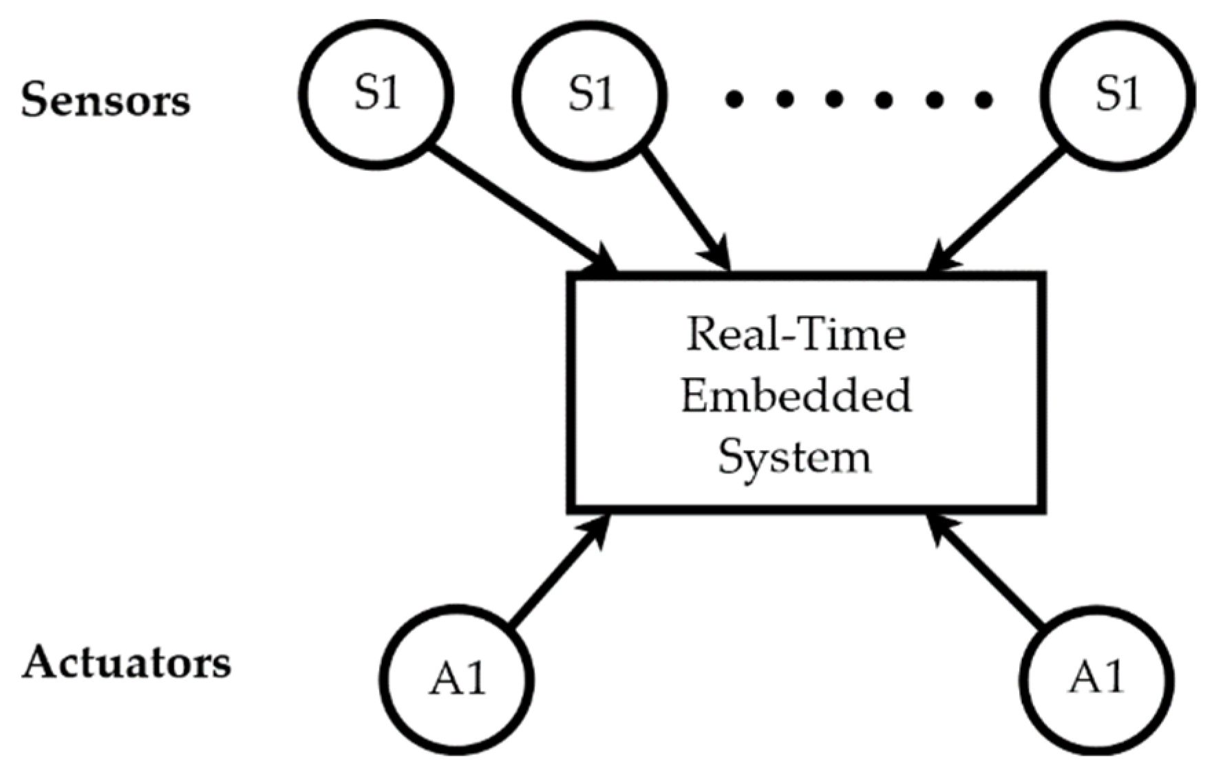
Embedded systems are computing systems with tightly coupled hardware and software integration that are designed to perform a dedicated function [
20]. The reactive nature of embedded systems is shown in
Figure 1. A reactive system must respond to events in the environment within defined time constraints. External events being aperiodic and unpredictable makes it more difficult to respond within a bounded time frame [
21].
Hard real-time embedded systems (
RTESs) refer to those embedded systems which require real-time behavior with for a missed deadline [
22]. The software part of an RTS is an application that runs either in stand-alone mode (bare metal) or scheduled as a task on a real-time operating system (RTOS). The hardware part includes one or more central processing units (CPU), memory elements, and input/output (I/O) devices with interrupt mechanisms to provide deterministic bounded responses to external events.
The term
timing anomaly refers to a situation where a local worst case does not entail the global worst case. For instance, a cache miss (the local worst case) may result in a shorter execution time than a cache hit due to scheduling effects [
3]. The
domino effect is a severe special case of timing anomalies that causes the difference in execution time of the same program starting in two different hardware states to become arbitrarily high [
13].
One of the metrics of microprocessor performance is the average number of clock cycles per instruction (
CPI), the lower the value the better the performance. Given a sample program with
instructions, the instruction count
for each instruction type
, and the number of clocks needed to execute instruction type
, CPI can be defined as shown in Equation (1).
CPI in conjunction with processor clock rate can be used to determine the time needed to execute a program [
17]. The classic 8051 CPU requires at least 12 cycles per instruction (CPI > 12) [
23], PIC16 takes 4 cycles or more (CPI > 4) [
24], but ** clocks to eliminate load and branch delays. The drawbacks of this approach are:
Incompatibility with optimization algorithms embedded in electronic design automation (EDA) tools.
No FPGA primitive support to implement the design.
Accessing memory after MUL instruction needs two cycles instead of one, and interrupt and events have a delay in some cases.
Difficulty reaching high clock speeds (e.g., 60 MIPS needs a 120 MHz oscillator).
5. Zipi8: A PicoBlaze Compatible Soft Core
In this section, the methodology behind transforming a PicoBlaze firm core to a soft core using vendor-independent primitive definitions (in VHDL) is detailed.
5.1. Primitive Conversion to Vendor-Independent VHDL
One of the primitives listed in the previous section is picked as an example: LUT6. The **linx Library Guide reads “LUT6 is a six-input look-up table (LUT), it can either act as asynchronous 64-bit ROM (with 6-bit addressing) or implement any six-input logic function” [
73]. A VHDL implementation must be written according to the extracted definition of the primitive.
Listing 1 shows one of the LUT6 instances used in the PicoBlaze core as an example. The ‘pc_mode2_lut’ is the instance name, and 0xFFFF_FFFF_0004_0000 is a 64-bit hexadecimal constant used as the initial value of the LUT6 primitive. I0, I1, I2, I3, I4, and I5 are inputs, and O is output signals.
First, a Boolean function minimization on the six-input logic function using the given 64-bit LUT value is performed. The minimization method can be either manual or automated, using algorithms such as the Espresso logic minimizer [
74]. Equation (2) shows the result of minimization of the six-input logic function LUT6(I5, I4, I3, I2, I1, I0) shown in Listing 1.
Listing 1: An example of LUT6 primitive instantiation used in the PicoBlaze core.
pc_mode2_lut : LUT6
generic map (INIT=>X"FFFFFFFF00040000")
port map (
I0 => instruction (12),
I1 => instruction (14),
I2 => instruction (15),
I3 => instruction (16),
I4 => instruction (17),
I5 => active_interrupt,
O => pc_mode (2)
);
After replacing the I0, I1, I2, I3, I4, I5, and O variables in Equation (2) with the name of signals connected to them, the exact equivalent vendor-independent VHDL implementation of LUT6 can be derived, as shown in Listing 2.
Listing 2: An example of vendor-independent VHDL implementation of LUT6.
pc_mode (2) <=
active_interrupt or
instruction (17) and
(not instruction (16)) and
(not instruction (15)) and
instruction (14) and
(not instruction (12));
The case for other primitives is the same. The vendor-independent VHDL implementation of the rest of the primitives, including “LUT6_2, FD, FDR, FDRE, XORCY, MUXCY, RAM32M, RAM256X1S”, can be found in
Supplementary S1, which includes the VHDL source code of all primitives in a **linx Vivado project.
5.2. Modular Conversion of PicoBlaze to Zipi8
The PicoBlaze VHDL source code has no modular structure. It is a module in a VHDL file with a long list of primitive instantiations connected via signals. To convert the design from a firm core (PicoBlaze) to soft core (named Zipi8 by the authors), it is sufficient to directly replace all the instances with vendor-independent VHDL equivalent code, as mentioned in the previous section. If, along the process, the related primitives are grouped into VHDL modules (based on the characteristic equation of flip-flops) and then transformation is performed, then complexity can be managed, human errors are minimized, and a modular design emerges. Additionally, the process provides better understanding of the internal architecture of the design.
The PicoBlaze core is transformed into 16 modules which use source code comments and original primitive names. The module names are listed below, and their source code can be found in
Supplementary S1:
arith_and_logic_operations;
decode4alu;
decode4_pc_statck;
decode4_strobes_enables;
flags;
mux_outputs_from_alu_spm_input_ports;
program_counter;
register_bank_control;
sel_of_2nd_op_to_alu_and_port_id;
sel_of_out_port_value;
shift_and_rotate_operations;
spm_with_output_reg;
stack;
state_machine;
two_banks_of_16_gp_reg;
x12_bit_program_address_generator.
The modules listed above and important signals between them are shown in
Figure 4. It is a simplified version of a fully detailed schematic that is available (in
Supplementary S2) in Encapsulated Postscript (EPS) format. To simplify the diagram, occasionally two or three related modules are combined. This is indicated by mentioning module numbers in parentheses. For example, the ‘Decoders’ module consists of three submodules: (2), (3), and (4). Both program memory and the processor share the same clock signal. Those modules which are synchronized with the clock are marked with a triangular symbol. The absence of a clock symbol indicates pure Combinatorial Logic (CL) (e.g., the ‘Operand Selection’ module).
5.3. Zipi8 Architecture
The important paths, such as the ‘data path’ and ‘instruction path’, are explicitly marked in
Figure 4. The allocation of two separate buses connected to two different memory blocks indicates a Harvard architecture [
56]. To explain the instruction execution mechanism of PicoBlaze, a sample program (Listing 3) with a branch instruction is manually traced.
Listing 3: A sample PicoBlaze program.
Start_at_0x000:
LOAD s0, 05 ;Loads value 05 into registers 0 – Mem. Location: 0x001
LOAD s1, 04 ;Loads value 04 into registers 1 – Mem. Location: 0x002
JUMP subprogram_at_01c ; – Mem. Location: 0x003
; ...
subprogram_at_01c:
ADD s1, s0 ; s1 <= s1 + s0 ; – Mem. Location: 0x01c
As shown in
Figure 5, the de-assertion of the
reset signal puts the processor into the
run state. In this state, the processor waits for the first rising edge of the clock that triggers an instruction fetch from memory location 0x000. The fetch results in the ‘Instruction Path’ bus (see
Figure 4) hold valid data (it is the first instruction, ‘LOAD s0, 05’, in Listing 3).
The instruction bus is connected to flip-flops in ‘Decoders’, ‘State Machine & Control’, ‘Flags’, and ‘Program Counter’ modules. When the second clock arrives, the instruction is decoded (sx_addr is set to 0 to select register s0, and the 05 constant value is placed on the instruction [7:0] bus, the kk instruction bitfield), the next state of machine is calculated, flags are set, and finally the program counter (PC) is incremented by one.
In the third clock cycle, the instruction at location 0x001 is fetched and the result of the ALU is written back into the register in parallel. This results in the s0 register holding the constant value 05. In the next clock cycle, the instruction at location 0x001 (which is ‘LOAD s1, 04’) is fetched.
As with previous instructions, the decode and execute stages happen in the next clock cycle, which sets the
sx_addr signal (see
Figure 4) to 1 and prompts the second ALU operand (
kk bitfield) to hold the constant value 04. In the next clock cycle, the processor writes back the result into the register bank, resulting in constant value 04 being stored in the
s1 register and, at the same time, the next instruction (‘JUMP subprogram_at_01c’) being fetched.
In the next cycle, the JUMP instruction is decoded and, instead of ‘pc = pc + 1’ and the next consecutive instruction being fetched, pc is set to a value of 0x01C, which is the jump target location. In the next cycle, the instruction at location 0x01C of program memory (‘ADD s1, s0’) is fetched. The ADD instruction is then decoded, and the ALU needs some time (ALU propagation delay) to perform the add operation. The result is ready before the rising edge of the next clock cycle arrives, when it will be written back into the s1 register, and so on. This manual execution tracing clearly shows the behavior of the PicoBlaze when it executes a branch instruction in two clock cycles.
Each original PicoBlaze instruction takes exactly two clock cycles (CPI = 2), making its ISA performance deterministic. This turns PicoBlaze into a suitable candidate for safety-critical real-time embedded systems [
38] if its performance can be improved without adding a pipeline or caches. In the next section, a new design is proposed that achieves CPI = 1 with PicoBlaze, resulting in significant performance improvement.
5.4. Zipi8 Verification
We use the
comparison method to verify the integrity of the Zipi8 core against the PicoBlaze. Flip-flop output signals have a one-to-one relationship in both cores. Therefore, the transformation process can be validated by probing signals at all output junctures of flip-flops in both cores and by using VHDL
assert statements to catch any discrepancies between them. Verification details and extra information on PicoBlaze to Zipi8 conversion can be found in [
18].
7. Zipi8 (CPI = 2) to DAP-Zipi8 (CPI = 1)
The first step is to set program memory BRAM to dual-port mode with the following settings:
Apart from address and instruction buses, two more buses named address2 and instruction2 are added to fetch an extra instruction on every rising edge of the clock. The original design updates the PC signal every two cycles based on control signal t_state(1) and is toggled every cycle.
By removing the
t_state(1) signal, the PC value is forced to be updated every clock cycle. The next step is to remove all D flip-flops (FDs) which take part in the construction of the two-stage pipeline. All modifications applied to all 16 modules of the Zipi8 core are listed in
Supplementary S4.
After applying the changes, a single-cycle processor is nearly achieved. It includes fetch, decode, and execution stages all in one cycle. However, the new design fails to calculate the correct next pc value if the processor state machine deviates from the normal flow (
pc =
pc_value + 1).
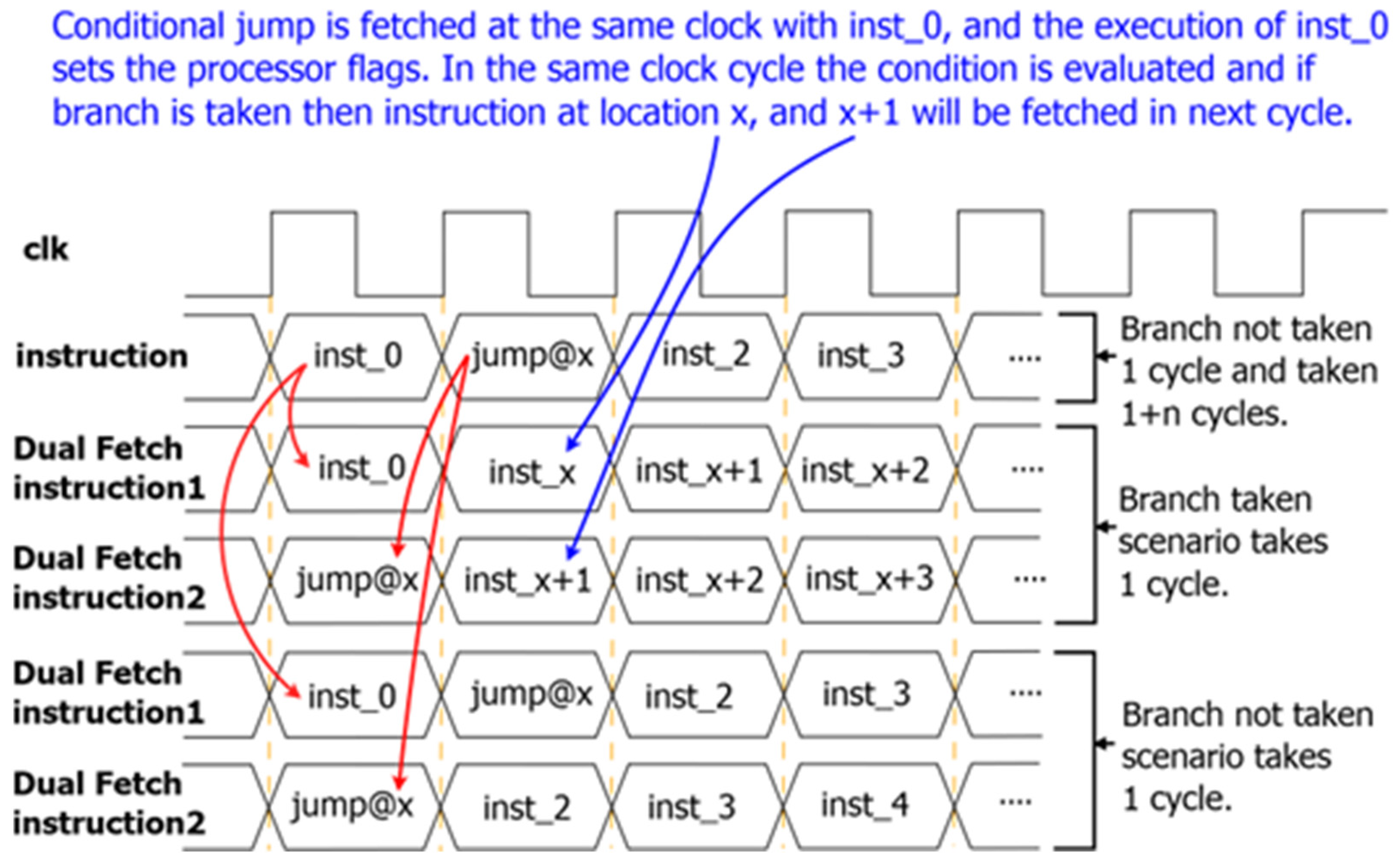
Figure 9 elaborates this failure when normal flow is disrupted by a branch instruction. Let us assume that an instruction at memory location 0x002 is a conditional jump to an arbitrary target memory address ‘x’. The processor fetches inst_0 and inst_1 from memory location 0x000 and 0x001 as normal. The PC value is then set to 0x002 and, in the next clock cycle, the jump@x instruction is fetched. As the design still needs two clock cycles to calculate the right
pc_value, the jump target address value propagates to
pc one clock cycle late and the instruction after the conditional jump (inst_3, which should not be reached by the processor and inst_2, is a jump and is taken) is then fetched wrongly. This is the inherent problem of branch instructions that leads to pipeline stalls as discussed earlier.
7.1. Adding the Dual Address Bus and Branch Prediction Circuit
The main idea behind the dual address bus branch prediction (DAP) circuit is to fetch two instructions per clock cycle by using a dual-port program memory block. This allows the circuit to predict the next PC value correctly by decoding the first fetched instruction in one clock cycle and then using the decoded signals in the execution step of the next clock cycle.
The schematic provided In
Figure 10 shows the Zipi8 modules which must be modified to accommodate the DAP circuit (added signals are in blue). Note that ALU, decoder, and SPM modules are not shown in this figure as these modules remain intact. The most important added signals are
instruction2 and
address2. They are connected to the second port of external program memory BRAM. The
address2 signal (derived by
pc2) holds the address of the second instruction and is always fetched in parallel with the current instruction (derived by
pc). Both
pc and
pc2 are generated by the ‘Program Counter’ module (module no. 7 and 16).
The second most important modification is the conversion of RAM32M primitives to dual-port instances in module no. 7, 16, and 13. This enables two locations of stack memory and registers (which are also memory) to be accessed instead of one location. This is achieved through simultaneous access to PORTA and PORTB of block RAMs on every clock cycle.
This is mandatory for prediction of the target address of instructions such as ‘return’, which uses the stack memory (using PORTB of the stack memory), or ‘call@(sX, sY)’, which uses the register banks (using PORTB of the register bank memory). sx_addrB and sy_addrB are connected to PORTB of the register memory BRAM, which makes simultaneous access to 2 out of 32 registers possible through PORTA and B.
Referring to
Figure 10, the
sxB and
syB signals are the output of BRAM’s PORTB in general-purpose register banks. The
push_stack2 and
pop_stack2 signals, alongside the
pc2 signal, are added to the PORTB of BRAM used in the ‘Stack’ memory module. These signals assist the prediction of correct stack pointer values and, consequently, the ‘Stack’ module can then set the correct ‘stack_memory’ value, as well as other necessary outputs.
Next is the addition of the
internal_reset_delayed signal to the ‘State Machine’ module. As can be seen in
Figure 9, this signal goes low one clock cycle earlier than the
internal_reset signal. This provides one extra clock cycle to the ‘Program Counter’ module for predicting the
pc2 value. The
carry_flag_value and
zero_flag_value (see
Figure 10) are simply the next values of the
carry_flag and
zero_flag signals calculated based on the execution of the current instruction. There are few internal signals of the ‘Flags’ module that are required to be routed out of the module for use as input to the ‘Program Counter’ module for prediction. In the original design, the ‘Register Bank Control’ module is responsible for producing
sx_addr and
sy_addr and depends on the
sx_addr4_value produced by the ‘State Machine’ module. The purpose of reusing ‘Register Bank Control’ and moving it into the ‘Program Counter’ module is to generate the
sx_addr [
4] signal. The core of the prediction mechanism is inside the ‘Program Counter’ module, which will be discussed in the next section.
7.2. Program Counter Module Modification
In the original PicoBlaze, the ‘Program Counter’ module is responsible for determining the next PC value in each clock cycle.
Figure 11 depicts the internal structure of the modified ‘Program Counter’ module. Analysis of PicoBlaze shows that the ‘Program Counter’ module receives the following signals as input:
The module then calculates the pc_value as output, which is then clocked to the PC. This constructs a simple Mealy state machine where the output depends on inputs and the current state of machine. The state machine then identifies the four necessary signals that must be present to calculate the next PC register value (pc_value signal).
At the heart of
Figure 11 we have ‘combinational logic (A)’, which receives the
pc,
register_vector,
pc_vector, and
pc_mode values and generates the
pc_value which is the next value of the PC register. This block is combinatorial and, in the original design, is constructed using LUT6, MUX, and XOR primitives. The exact duplication of this block is named ‘combinational logic (B)’ and is used to generate the
pc2_value signal. The inputs to combinational logic (B) are derived from exact duplication of ‘(16) 12-bit Address generation’ and ‘(3) Decoding for program counter and stack’ modules. Instead of
instruction,
sx,
sy,
carry_flag, and
zero_flag signals, the
instruction2,
sxB,
syB,
carry_flag_value, and
zero_flag_value signals drive their inputs. This produces the
pc2_value signal which is the potential guessed value for the next PC register value.
Three modes are defined based on the two fetched instructions A and B, and the details of how the final value of the PC register is calculated and set are then discussed. The modes are:
‘Normal’ mode: instructions A and B do not modify the PC register and both are not JUML, CALL, or RETURN instructions.
‘Guessed value is used’ mode: instruction B modifies the PC register but instruction A does not.
‘Illegal’ mode: instructions A and B both modify the PC register.
In the original design, the pc_value signal (the next value of the PC register) is directly connected to the ‘pc_fd’ flip-flop. The design is modified by adding the ‘pc_mux’ multiplexer before the ‘pc_fd’ flip-flop, which selects the correct predicted pc_value based on three signals ordered from high to low priority:
internal_reset;
guessed_value_used;
pc2_mode.
If the internal_reset signal is high, regardless of other multiplexor selectors, the pc will be set to zero (processor reset). If the internal_reset signal is low, then the processor is in running mode and the guessed_value_used signal will be checked. When guessed_value_used is high, it means the processor is in ‘Guessed value is used’ mode, which indicates that current instruction A has modified the PC register and, consequently, the guessed value has been used already; therefore, the next valid instruction will be in the ‘pc + 1’ memory location. Note that addition of this multiplexor increases the critical path of the processor.
It should be noted that it is illegal to have two consecutive instructions which both modify the PC register. Therefore, if the current instruction has modified the PC, the assumption is that the next one will not; therefore, incrementing the PC by one is always the correct way to advance the processor state machine. When guessed_value_used is low, it means the processor is in ‘Normal’ mode, which indicates that the current instruction does not modify the PC register.
The next step is to investigate the next instruction that has already been fetched and decoded. The binary value ‘0b001’ for the pc2_mode signal indicates that the next instruction will not modify the PC register and, therefore, that pc_value is the next value of pc. The binary value ‘0b011’ for the pc2_mode signal indicates that the next instruction is a RETURN instruction; therefore, pc_value must be discarded and, instead, the return address fetched from stack in advance (pc2_value) must be used as the next pc value. The binary value ‘0b110’ for pc2_mode indicates that the next instruction is a ‘CALL@(sX, SY)’ instruction and that the next value of pc must be a concatenation of the content of [xS,xY] registers, both of which are fetched from the register bank in advance and placed on the pc2_value signal.
In
Figure 11, the
pc2_mux and
pc2_rst_mux signals select the next value for the
pc2 signal. If the
internal_reset_delayed signal is high (processor reset), then
pc2 will be set to zero; otherwise, the next value of
pc2 will be either
pc2_value (Normal mode) or
pc2_value + 1 (not Normal mode).
The last module that needs to be discussed here is the ‘Register Bank Control’ module, which outputs the
sx_addr [
4] signal. As shown in
Figure 11, input signal
sx_addr [
4], alongside the
shadow_bank and i
nstruction2 signals, sets the output signals
sx_addrB and
sy_addrB. These two output signals hold values destined for PORTB of the register bank’s memory.
To summarize the modification technique presented above, all memory blocks are converted to dual-port mode to fetch two instructions in parallel. The minimum logic in the original decoder is then replicated (‘combinational logic (A) and (B)’) to produce signals for prediction circuitry that result in removal of branch and load delays.
7.3. Stack Module Modification
In the original PicoBlaze design, the ‘Stack’ module is responsible for producing
zero_flag,
carry_flag,
bank, and
special_bit signals alongside of the
stack_memory signal, as detailed in
Supplementary S2. They depend on
push_stack and
pop_stack input signals set by decoding circuitry. The current value of the internal signal
stack_pointer drives the ADDRA port of BRAMs that is used as stack memory. The memory content the
stack_pointer points to holds the return value address.
For example, if the processor executes a RETURN instruction, then a pop_stack signal will be asserted which prompts the ‘Stack’ module to decrement stack_pointer by one. This will put the memory content of “stack_pointer − 1” on the stack memory output data bus, which in turn recovers the flags, bank, and pc register values. When a CALL instruction gets executed, the push_stack signal is asserted, which prompts stack_pointer to be incremented by one (“stack_pointer + 1”). Next, the WE signal will be set to a high value so the current flags and pc value can be saved into stack memory.
The modification of the original design starts by enabling the dual-port option for BRAMs used as stack memory. The push_stack and pop_stack inputs must be removed as they are calculated one clock cycle late (PicoBlaze uses two clock cycles, and these two signals are used in the second clock cycle). These two input signals are replaced by push_stack2 and pop_stack2 signals, which are generated by prediction circuitry in advance. They detect whether the current instruction is a RETURN or a CALL, which prompts a pop from stack memory or a push into stack memory, respectively.
The next step is the removal of all LUT, MUX, XOR, and FD primitives and redesign of the ‘Stack’ module to accommodate prediction circuitry, which is shown in
Figure 12. The
stack_pointer signal is connected to the ADDRA port, and a series of multiplexors decide whether the pointer must be incremented or decremented based on the values of
push_stack2 and
pop_stack2. The
stack_pointer is connected to the ADDRB port and always points to the location of “
stack_pointer − 1”.
This makes the content of memory locations at stack_pointer and “stack_pointer − 1” available at any given clock cycle through stack_memory1 (memory content on ADDRA) and stack_memory2 (memory content on ADDRB) signals. The two multiplexors, with pop_stack2 as their selector, decide the final value of the flag, bank, and stack_memory signals. Note that the WE pins of both BRAMs are permanently pulled up (connected to Vcc), which forces a continuous write on every clock cycle at the memory location pointed to by the ADDRA value.
With addition of the circuit mentioned above, the processor constantly writes the status of flags and the current PC register value into stack memory at every clock cycle (constant push). At the same time, it constantly reads two locations from stack memory pointed to by the stack pointer and the stack pointer subtracted by one. The prediction circuit drives the processor to pop the stack (decrement the stack pointer by one and use the output of PORTB to recover the PC register value and flags through the pop_stack2 signal) or continue normal operation (the stack pointer will be intact and the output of PORTA will be used). In case of a push, the processor just needs to increment the pointer by one (triggered by push_stack2), as writing to stack memory is already performed on every clock cycle regardless of whether the push_stack2 signal is asserted.
8. Resource and Power Utilization
Table 3 compares the resource utilization of our proposed DAP-Zipi8 with CPI = 1 with that of Zipi8 with CPI = 2 and the original PicoBlaze. Referring to
Table 3, the maximum clock frequency obtained with the **linx Zynq UltraScale+ MPSoC ZCU104 Evaluation Kit was 369.041 MHz, which is attributed to the original **linx PicoBlaze.
The conversion of a firm-core PicoBlaze to a soft-core Zipi8 is essential if we want to modify the design. The converted soft core, named Zipi8, can achieve a maximum frequency of 357.509 MHz (=2.86% decrease) and an increase in LUT count from 122 to 157 (28.69% increase). This is the cost (increase in logic area) that must be paid to make the register transfer level (RTL) HDL source code of PicoBlaze available for modification.
The dual-fetch technique, explained previously in conjunction with dual-port memory, and the addition of dual-address bus prediction circuitry yields a new processor that is named DAP-Zipi8, which has a LUT count of 305 (94.27% increase compared to Zipi8) and a maximum frequency of 224.022 MHz on the **linx ZCU104 development board. Note that the removal of flip-flops between decoder and execution stages results in a reduction in total register count from 74 to 49 (see
Table 3).
Although the DAP-Zipi8 critical path has increased (which results in lower achievable maximum clock frequency), CPI is reduced from two to one (50% decrease). Considering processor performance in terms of million instructions per second (MIPS), the calculation of MIPS for Zipi8 (CPI = 2) is shown in Equation (3).
For DAP-Zipi8, the calculation is shown in Equation (4).
MIPS is not an accurate metric to compare the performance of processors with different ISAs. For example, comparison of Intel versus ARM versus PicoBlaze using the MIPS metric is incorrect. In those cases, benchmarks from Dhrystone, the Embedded Microprocessor Benchmark Consortium (EEMBC), or the Standard Performance Evaluation Corporation (SPEC) should be used, as instructions in different ISAs might perform different amounts of work. For example, one ISA might have an instruction that performs a simple addition operation, while another ISA might have special digital signal processing (DSP) instructions that perform addition and multiplication as one combined instruction. In this paper, the modified PicoBlaze (DAP-Zipi8) and PicoBlaze itself both have the same ISA and are compared against each other. This justifies employment of the MIPS metric as a meaningful performance indicator [
17].
As shown in
Figure 13, a 25.31% performance improvement for the DAP-Zipi8 processor (increase from 178.75 to 224 MIPS) is achieved without considering the impact of mandatory NOP instructions (inserted to avoid invalid examples of the design).
Figure 14 shows four programs that were executed on both PicoBlaze and DAP-Zipi8 cores and their measured execution times (left side
y-axis). On the
x-axis, the ‘state_machine’ label refers to a complex finite state machine (FSM) that is used to control 1024 PicoBlaze cores on a single FPGA chip (XCZU7EV-2FFVC1156). The FSM is written by the authors and follows the work presented in [
75]. It is an RTES application that uses a myriad of cores for the adaptive routing and serving of swarms of incoming network traffic (miniature web servers running on PicoBlaze instances). Utilizing a PicoBlaze core as an FSM controller is common and the detail of this implementation, though out of the scope of this article, will be published in another paper. Note that this state machine is the main application of our proposed architecture, and it is not executable on indeterministic processors (processors with a pipeline or caches) as it expects programs to be executed in an exact predetermined number of clock cycles. It is noteworthy that the worst-case response time to external interrupts in this state machine is just three clock cycles using DAP-Zipi8 versus five cycles in the original PicoBlaze.
To avoid the invalid case (‘Illegal’ mode as defined in
Section 7.2) where two consecutive conditional jump instructions are present, a NOP instruction is inserted in between of jump instructions. A program in the final pass of compilation scans program opcodes and inserts a NOP instruction whenever two consecutive branch instructions are discovered.
In
Figure 14, the negative impact of added NOP instructions on performance for all algorithms is shown. The algorithms used in the benchmark are listed below:
PicoTETRIS [
76]: a Tetris game written in PicoBlaze assembly language.
An IEEE-754 64-bit floating point arithmetic library [
77].
A matrix multiplication algorithm written in PicoBlaze assembly language.
A state machine controller that manages multiple cores by implementing a complex FSM used to controlled 1024 PicoBlaze cores on an FPGA in real time.
The added NOPs increase the total instruction count (right-side
y-axis in
Figure 14 which is labelled “Instruction Count Increase after Added NOPs”) per algorithm. The percentage increase is shown with the black bar along the right-side
y-axis. Although the number of NOP instructions increased by around 1% (2.42% in the case of PicoTETRIS), their impact was quite significant. It reduced the performance gain from the initially obtained 25.31% down to 18.28~19.49%, as reported in
Figure 14.
Power consumption was measured using the **linx Vivado v2021.1 ‘Power Report’ facility for all three cores at both 100 MHz clock frequency and maximum achievable clock frequency. The total FPGA on-chip power consumption for all cores was 722~737 mW, which is divided into static and dynamic power. Static power was fixed at 615 mW and was FPGA device dependent. Total dynamic power consumption was 107~122 mW. A large portion of dynamic power was used in memory block RAM, clock generation circuitry, and other support modules. The portion of dynamic power that was used by cores is reported in
Table 4. It shows a 42.86% power increase (against 25.31% performance gain) in DAP-Zipi8 when running the cores at their maximum frequency.


