3.1. Variability in FETs with Single SWCNT
Performance variation in FETs with single s-SWCNT arises from the variation in
d, contact and gate metals’
ΦWF,
Lch,
Tox (oxide thickness), and interface and oxide defects from one FET to another. For FETs with
Lch>µm, variation in
d can give rise to several orders of magnitude change in
Ids, as shown in
Figure 7a for small
Vds = −50 mV. One can simulate such transfer characteristics for different
d (dashed lines in
Figure 7a) by considering the conductance of the FET (
Gds) as a series combination of conductances of s-SWCNT (
Gss; see Ref. [
44] for appropriate expressions) and contact (
Gc =
Gc0Tc; where
Tc is the transmission probability of carriers near the source/drain contact) with components from both electron (e) and hole (h),
i.e.,
and hence, calculate
Ids using
Ids =
Gds ×
Vds. Simulated results for 0.6 nm <
d < 1.75 nm are consistent with measurement at
Vg <
Vt, where
Gss dominates
Gds. The differences in the region of
Vg >
Vt, where
Gc dominates
Gds, partly reflect variation in the fixed component of
Gc [
80] that is not considered in simulation and also reflect
Ids measurement limitation set at ~pA. Plots of diameter dependence of
Ion (
≡Ids @
Vg −
Vt = −1V,
Vds = 50 mV), maximum transconductance
Gm,max (≡max |
∂Ids/∂Vg|), and
Vt (
Figure 7b) provide additional detail about the origin of performance variation in s-SWCNT FET. At large diameters, when the transmission of carriers through the Schottky barrier near the contacts is unity, variation of
Ion ~
d and
Gm,max ~
d2 originates from the diameter dependence of
μeff in s-SWNTs [
5,
81,
82]. Similarly, variation of
Vt (≡
Vg @ |
Ids| = |
Ids,max|/100) with
d follows that of
Ion. At small diameters, non-linear dependence of transmission through the contact Schottky barrier leads to a non-linear variation in
Ion,
Gm,max, and
Vt with
d.
Simulated
Ion,
Gm,max, and
Vt distributions (calculated using diameter distribution of
Figure 7c and variations of
Ion,
Gm,max, and
Vt vs. d from
Figure 7b) suggest good consistency with respective measurements (
Figure 7d–f). Similar to the diameter distribution of
Figure 7c,
Ion distribution fits log-normal statistics, except near the lower tails of the distribution where transport through the contacts’ Schottky barrier with
Tc < 1 dominates
Ids. Measured
Vt − <
Vt> distribution (where <
Vt> is the average of the distribution) is wider than the simulated one due to the extra contributions from defects [
16,
83] and gate
ΦWF [
84,
85] variations that is not considered in the simulation. Passivation of SWCNT interface using hydrophobic self-assembled monolayers (SAMs) can tighten the
Vt distribution by reducing hydroxyl (–OH) group related interface defects [
86].
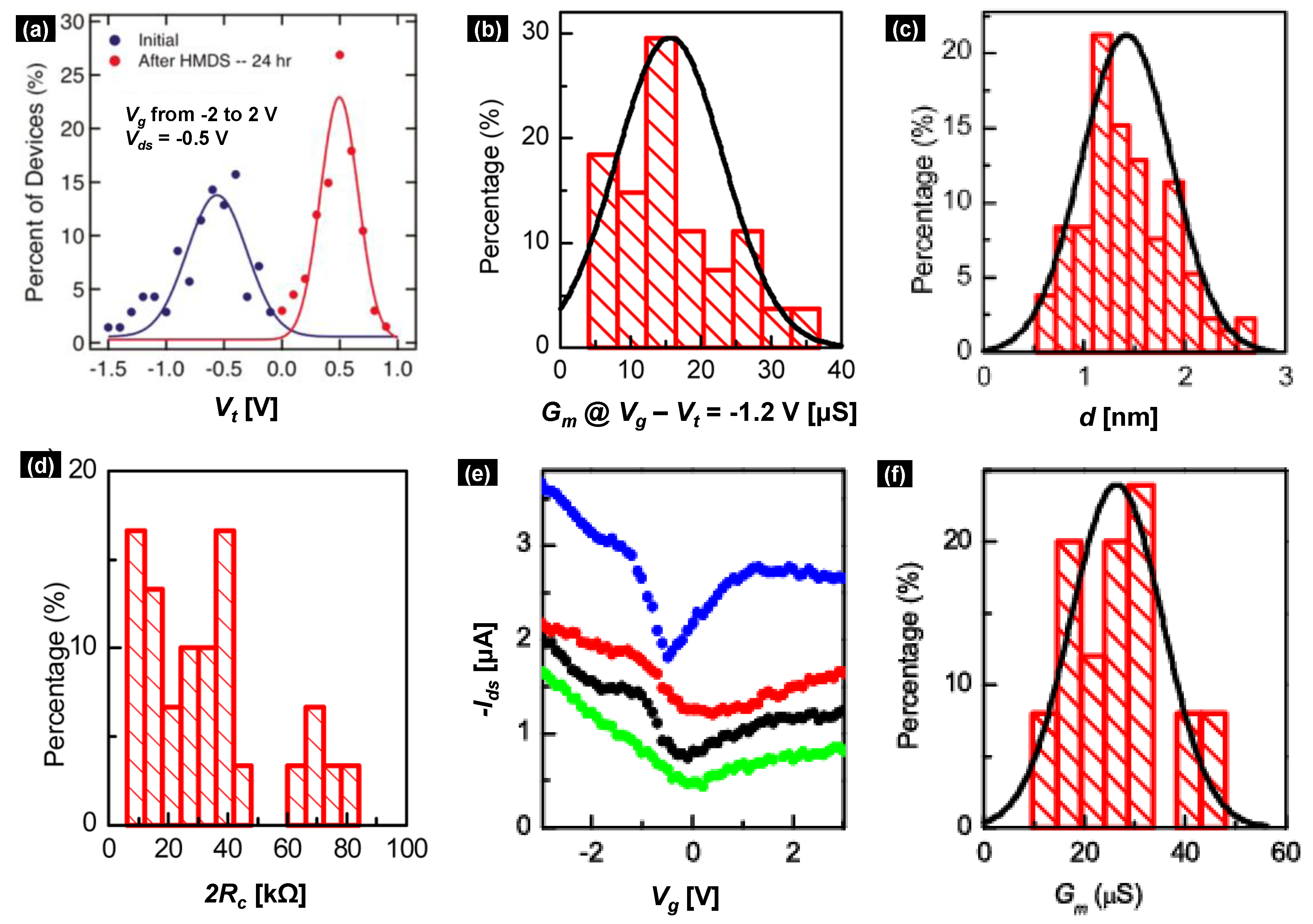
Figure 8a demonstrates utility of such SAM-based approach for reducing
Vt distribution, where
Lch << µm s-SWCNT FETs are made using solution-processed SWCNTs and passivated with hexamethyldisilazane (HMDS). As in CVD-grown s-SWCNTs, distribution in
Gm (
Figure 8b) for such solution-processed s-SWCNT FETs follows that of diameter (
Figure 8c). In addition, contact resistance
Rc = 1/
Gc in such small
Lch s-SWCNT FETs plays a dominant role in transport. Distribution of
Rc (
Figure 8d) arises from variations in
Tc with
d [
28] and also from variations in the contact’s
ΦWF. In contrary, FETs with m-SWCNT and similar
Lch have tighter
Rc distribution [
28]; however, they still suffer from variations in
Ids (
Figure 8e) and, hence,
Gm (
Figure 8f). Since m-SWCNTs are unattractive for high performance electronics applications requiring high
Ion/
Ioff, parametric variations in m-SWCNT FETs are not well studied.
3.2. Variability in FETs with Multiple SWCNTs
Similar to single SWCNT-FETs, performance variation in FETs with multiple SWCNTs originates from variations in
d,
ΦWF,
Lch,
Tox, and defects [
87,
88,
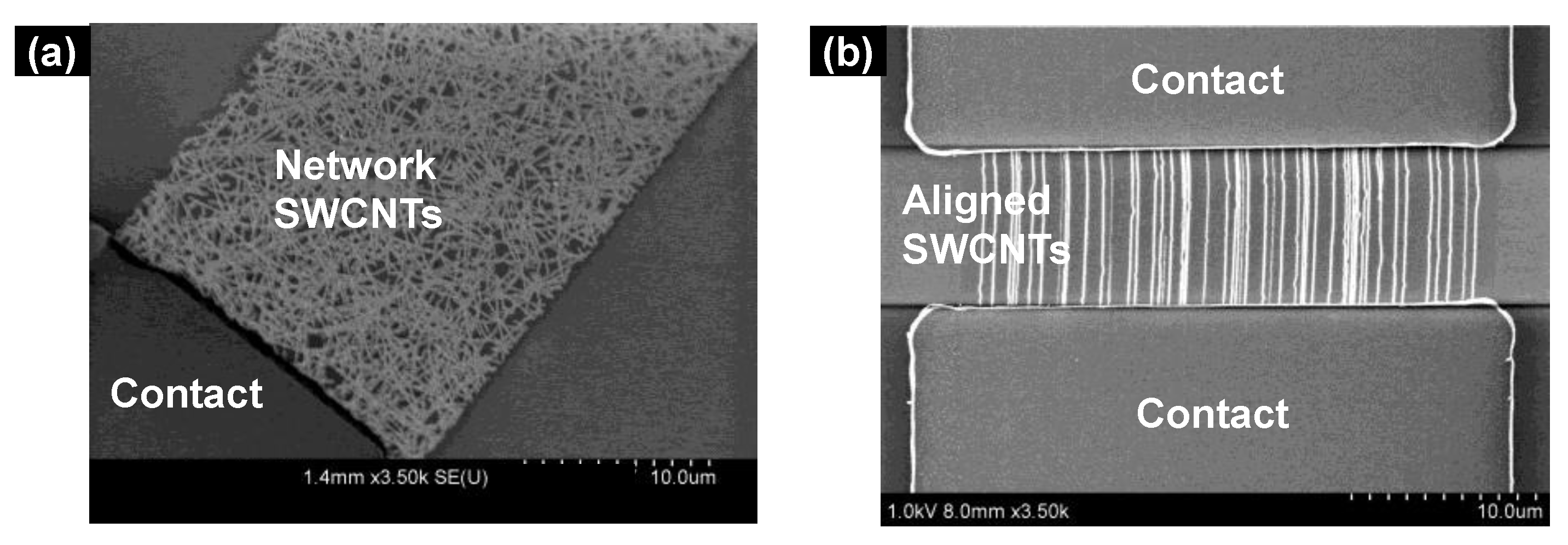
89]. A simple translation of single SWCNT-FET analysis to multiple SWCNT-FET; however, they cannot explain related variations, mostly because of the added complexity coming from variations in the arrangements and types of multiple SWCNTs bridging source/drain contacts. Multiple SWCNT FETs can have random network or aligned SWCNTs with varied density of m- and s-SWCNTs, a wide range of variations in the orientation of SWCNT and its crossings (especially for network SWCNT FET), and a wide distribution in
d. This section discusses performance variation in aligned array SWCNT-FETs that have significant promise for high performance device applications. Such FETs have negligible variation in SWCNT’s orientation [
77] and also have negligible SWCNT crossings (
Figure 6b). For a discussion on variabilities coming from SWCNT’s orientation and crossings, which are more relevant for network SWCNT-FETs, please refer to Ref. [
41].
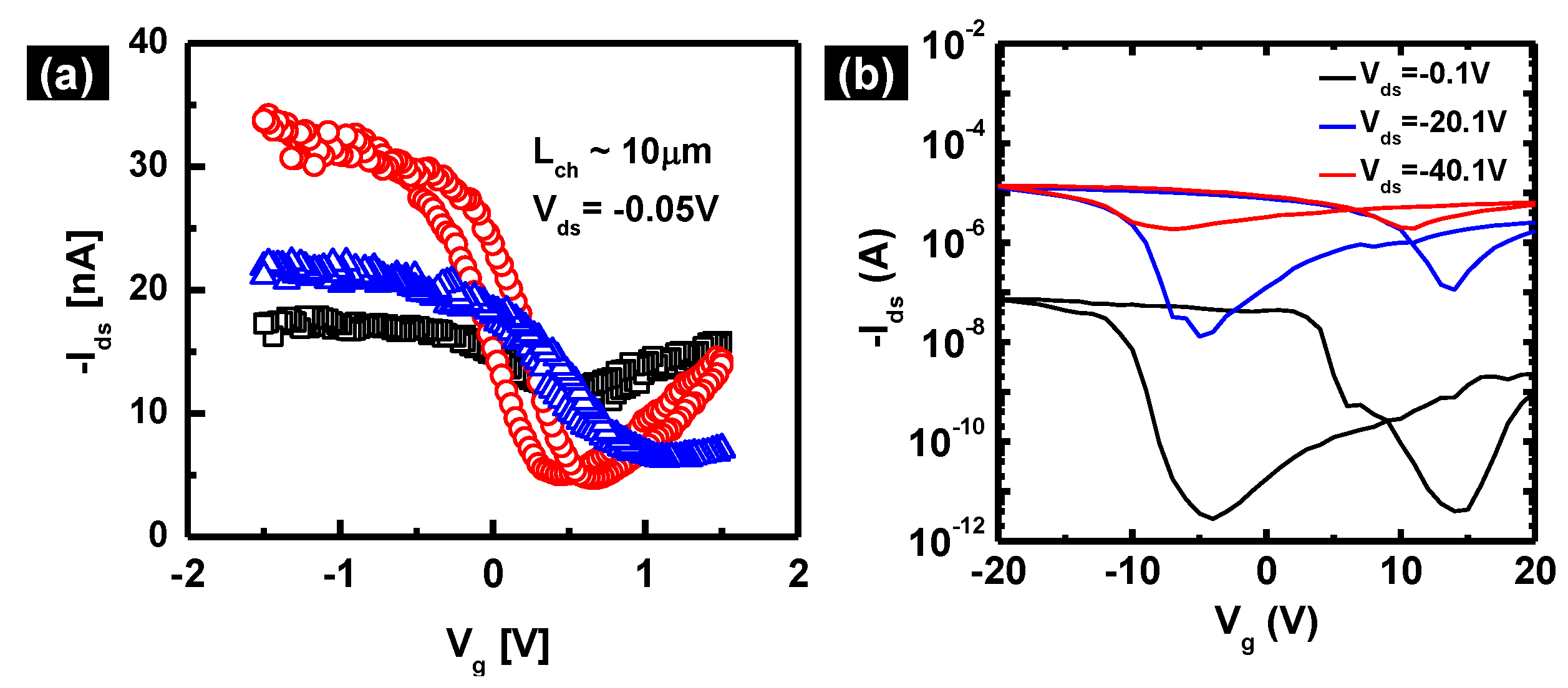
Figure 7.
(
a) Measured
Ids vs. Vg −
Vt (
Vt ≡
Vg @
|Ids| = |Ids,max|/100) characteristics for single s-SWCNT FETs (
Lch ~ 10 μm,
Vds = −50 mV) is within the simulated results for
d = 0.6 nm and
d = 1.75nm FETs. (
b) Simulated
Ion (≡|
Ids|@
Vg −
Vt = −1 V, V
ds = −50 mV),
Gm,max (≡max(∂
Ids/∂
Vg)), and
Vt vs. d for s-SWCNT FETs. (
c) Diameter distribution that is used to simulate performance distributions of s-SWCNT FETs in (
d–
f). Measured distributions of (
d)
Ion, (
e)
Gm,max, and (
f)
Vt for s-SWCNT FETs agree well with the simulated distributions (insets). For (
f), <
Vt> is the average of
Vt distribution. These figures are reprinted with permission from Ref. [
44]; © 2012, AIP Publishing LLC.
Solution-processed SWCNTs that are widely used for fabrication of FETs with network and partially aligned SWCNTs have yet to reach the target of 100% chiral selectivity. Some of the resultant FETs, therefore, have high on/off ratios when SWCNT density within the FET is low [
35,
46]. On the other hand, high performance electronics demand the availability of CVD-grown SWCNTs that always come with a mixture of m- and s-SWCNTs and require the application of post-processing techniques (e.g., electrical breakdown [
79], gas-phase reaction [
90], thermo-lithography [
54]) for having high on/off ratio in multiple SWCNT FETs. In some cases, application of post-processing techniques like electrical breakdown [
79] and gas-phase reaction [
90] also leads to unwanted removal of s-SWCNTs and, hence, performance degradation or even transistor failure [
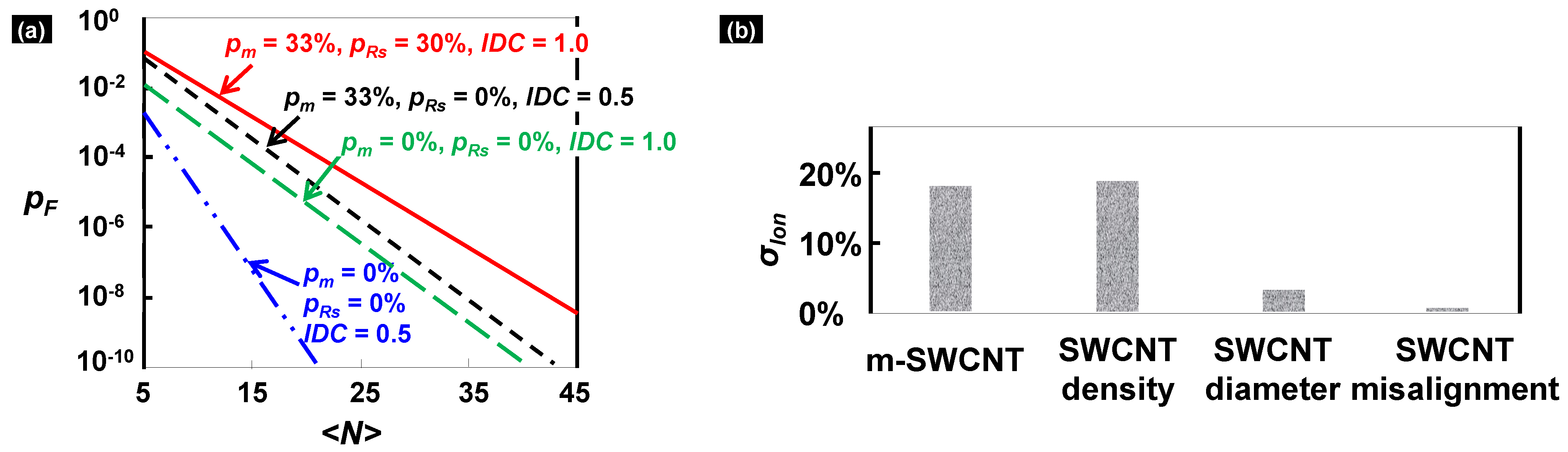
91]. Considering
pm as the probability of a single SWCNT in the FET being metallic,
pRs as the probability of s-SWCNT being removed via post-processing,
IDC as the index of dispersion in SWCNT count within the FET, one can simulate the failure probability (
pF) for FETs with aligned SWCNTs at different SWCNT densities (
Figure 9a). Such analysis, however, ignores a well-known aspect of ‘inferential statistics’ [
92],
i.e., the distributions of SWCNT density and
d in macro-scale (population distributions) is not always same as the distributions in micro-scale (sample distributions). As such, performance variability from diameter variations were expected to diminish for high density multiple SWCNT FETs via statistical averaging [
25,
41,
91], making SWCNT density and m-SWCNT’s presence as the major contributors to performance variations (
Figure 9b) [
91].
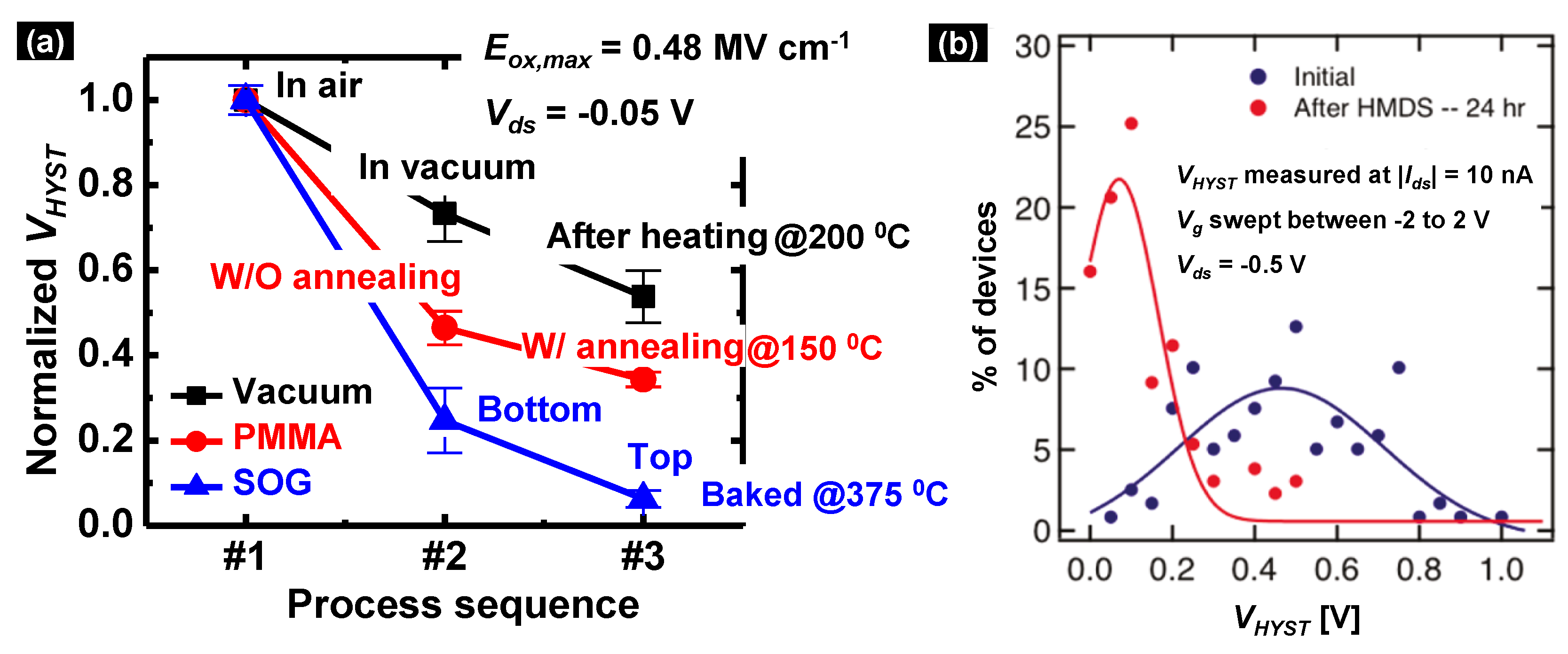
Figure 8.
(
a) Treatment of hexamethyldisilazane (HMDS) for 24 h narrows the
Vt distribution significantly.
Vg was swept from −2 V to 2 V for p-type, solution-processed s-SWCNT FETs during this measurement. Measured (
b)
Gm distribution and (
c) diameter distribution for similar solution-processed, s-SWCNT FETs that has small channel length (
Lch = 150 nm). (
d) Extracted contact resistance (
Rc) distribution for
Lch = 150 nm, solution-processed s-SWCNT FETs. (
e) Transfer characteristics and (
f)
Gm distribution for solution-processed, m-SWCNT FETs. (
a–
c) and (
d–
f) are reprinted with permission from Refs. [
28] and [
86], respectively; © 2012 American Chemical Society.
We performed a comprehensive experimental and theoretical study on FETs with aligned array SWCNTs [
44] and ruled out the presence of statistical averaging in aligned-array SWCNT-FETs.
Figure 10a plots distribution of
Ion (measured at a
Vg − Vt = −1 V) for aligned array-SWCNT FETs having
<N> ~ 11 SWCNTs, where
<N> =
<ρ>W is nominal number of SWCNT within the FET,
W is the channel width, and
<ρ> is the average SWCNT density on the substrate per µm across the length of the nanotubes. Since variation in
Ion follows Poisson statistics [
44], we account for changes in
µIon (that arises from variation in sample preparation) from one set of array-SWCNT FET to another by dividing the standard deviation of
Ion/
<N> (
σIon) with √
µIon (where
µIon is the average of
Ion/
<N>). Calculated
σIon/
õIon, normalized with respect to the same value measured for FETs with single SWCNT, shows a small reduction with the increase in
<N> (
Figure 10b). If the diameter and density distributions of SWCNT for each array-SWCNT FETs (sample distribution) were the same as the wafer-level distribution (population distribution) of these parameters, as per central limit theorem [
92], the normalized standard deviation should have reduced as 1/√
<N> due to statistical averaging. The existence of deviation from 1/√
<N>, therefore, suggests significant variations in SWCNTs’ density and diameter across the wafer, as was confirmed via extensive atomic force microscopy (AFM) at different locations over a macroscopic area of ST-cut quartz substrate that had CVD-grown aligned arrays of SWCNTs [
44].
Figure 9.
(
a) Variation in failure probability (
pF; defined as probability of having no s-SWCNT within the FET) of m-SWCNT removed (via post-processing) aligned-array SWCNT-FETs with <
N> (defined as the average number of SWCNTs within the FET before post-processing). Simulation is performed for different values of
pm (defined as the probability of having m-SWCNT within the FET before post-processing),
pRs (defined as the probability of s-SWCNT removal via post-processing), and
IDC (index of dispersion in SWCNT count). (
b) Different variation sources like the presence of m-SWCNT before post-processing, SWCNTs’ density, diameter, and misalignment contributes differently to the overall variation in standard deviation of
Ion (
σIon). Simulation suggests that the presence of m-SWCNT and density distribution are the key variability sources in SWCNT FETs. These figures are plotted using data from Ref. [
91].
To clarify the differences between measured
σIon/√µIon and expected 1/√
<N> dependency, measured diameter and density variations across the wafer are used first to calibrate the variations measured at the microscopic level (
i.e., electronic properties of single-SWNT-FETs, as discussed in
section 3.1). Later, the rules of “inferential statistics” [
92] is used to analyze variations at the macroscopic level (
i.e., for array SWCNT FETs). Here, density variation is eliminated by counting the number of SWCNTs (
N) for each array-SWNT FET and then using (
Ids/N) −
Vg characteristics for standard deviation calculation. Even after accounting for density variation, calculated
σIon at different
<N> (normalized to its value for
<N> = 1) shows significant deviation from 1/√
<N> scaling (
Figure 10c). Such deviation suggests SWCNT density variation as a minor contributor to performance variation, thus contradicting the results of Refs. [
25,
41,
91]. Finally,
Ids-
Vg characteristics of array-SWCNT FETs are simulated for different
<N> by considering experimentally calibrated diameter dependence of single-SWCNT FETs’s
Ids-
Vg characteristics (
Figure 7a) and measured (wafer-scale) density, diameter distributions of SWCNT.
Figure 10c,d show normalized standard deviations of
Ion (
σIon) and
Gm,max (
σGm), as simulated for different
<N> and their comparison to measured quantities. Since the sample sizes in measuring the standard deviations were small (~17–35), simulated standard deviations show a range of magnitudes for similar sample sizes within which the measured data points fits in. (The simulation framework [
44], used for calculating
σIon and
σGm of array-SWCNT FETs, neglects contributions from m-SWCNTs. However, the procedure is suitable for demonstrating the importance of wafer-level variations in diameter and density).
Figure 10.
(
a) Distribution of
Ion among array-SWCNT FETs with mean SWCNT density
<N> ~ 11. (
b) Normalized standard deviation of
Ion (
σIon)
vs. <N> deviates from 1/√
<N> scaling or central limit theorem. Normalized (
c)
σIon and (
d)
σGm for array-SWCNT FETs, where the effect of SWCNT density variation is removed by counting
N for each FET and then calculating the standard deviations using
Ids/N–
Vg characteristics of each FET. Variations in
σIon and
σGm still differs from 1/√
<N> and required the consideration of wafer-scale diameter distribution for matching experimental trends via detailed simulation. Figures are reprinted with permission from Ref. [
44]; © 2012, AIP Publishing LLC.
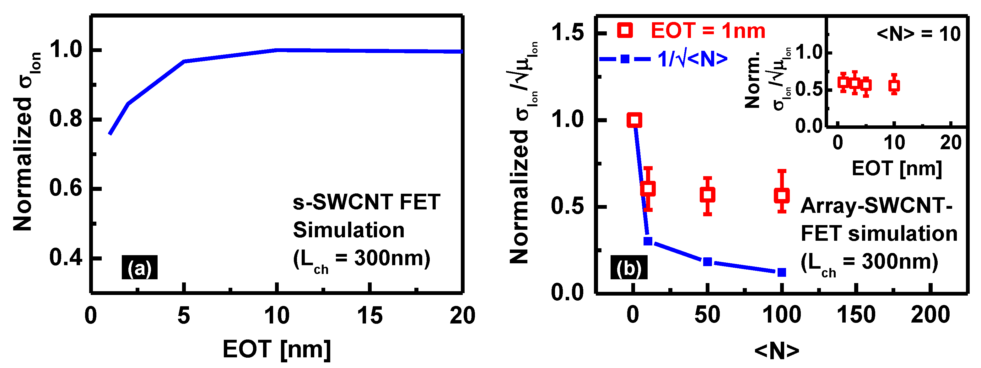
Recently, use of smaller equivalent oxide thickness (
EOT ≡
εSiO2/εHKTox; where
εSiO2,
εHK are dielectric constants of SiO
2 and high-κ dielectrics, respectively) has been shown to reduce the performance variation in FETs with single s-SWCNTs [
93]. Decreasing
EOT reduces the width of the Schottky barrier near the SWCNT and source/drain junction [
57] and removes the long negative tails in the
Ion distribution [
44]. Moreover, as
Lch approaches the carrier mean-free path of SWCNT,
Ids saturates for large diameter SWCNTs and hence diameter dependence of
Ids is less pronounced [
44]. Both these effects are studied by simulating small-scale array-SWCNT-FETs with
EOT ~ 1 nm and
Lch = 300nm. (Here, simulated
Ids-
Vg [
44] is calibrated with measurements of Ref. [
63]). Simulation suggests a decrease in
σIon for FETs with
<N> = 1 with decreasing
EOT (
Figure 11a). However, at larger
<N>, neither
EOT nor
Lch scaling could improve the statistics because the effects of variations in density and diameter remain significant (
Figure 11b). Therefore, narrowing diameter and density distributions are identified as the main areas for improvement via advanced growth and/or purification techniques to reduce performance variation in multiple-SWCNT FETs.
Figure 11.
(
a) Oxide scaling of s-SWCNT FET reduces
σIon (normalized by its value at equivalent oxide thickness (
EOT = 20nm), as observed in Ref. [
93]. (
b) Normalized
σIon (
i.e.,
σIon/
σIon,<N>=1) differs from 1/√<
N> scaling for
EOT = 1 nm array-SWNT FETs and show negligible effect of oxide scaling at fixed
<N> (inset). Figures are reprinted with permission from Ref. [
44]; © 2012, AIP Publishing LLC.


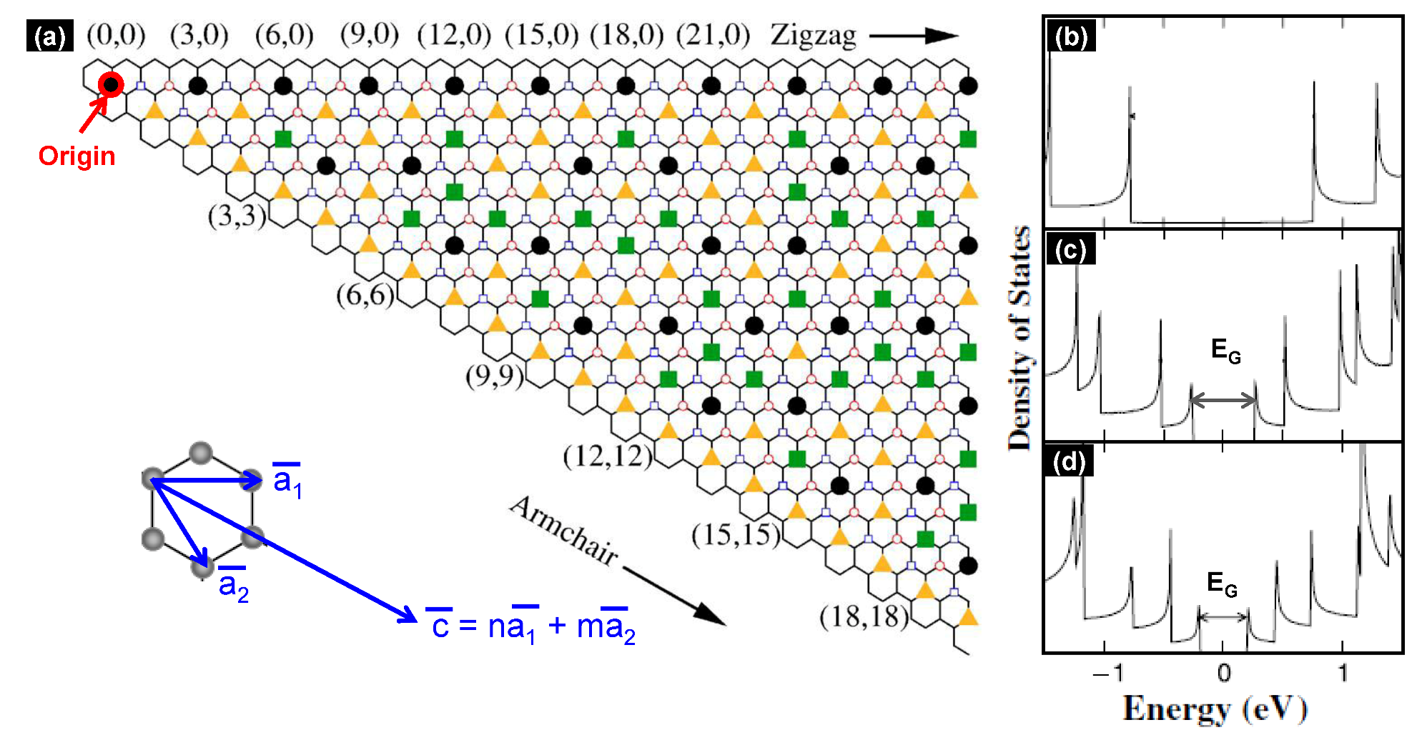
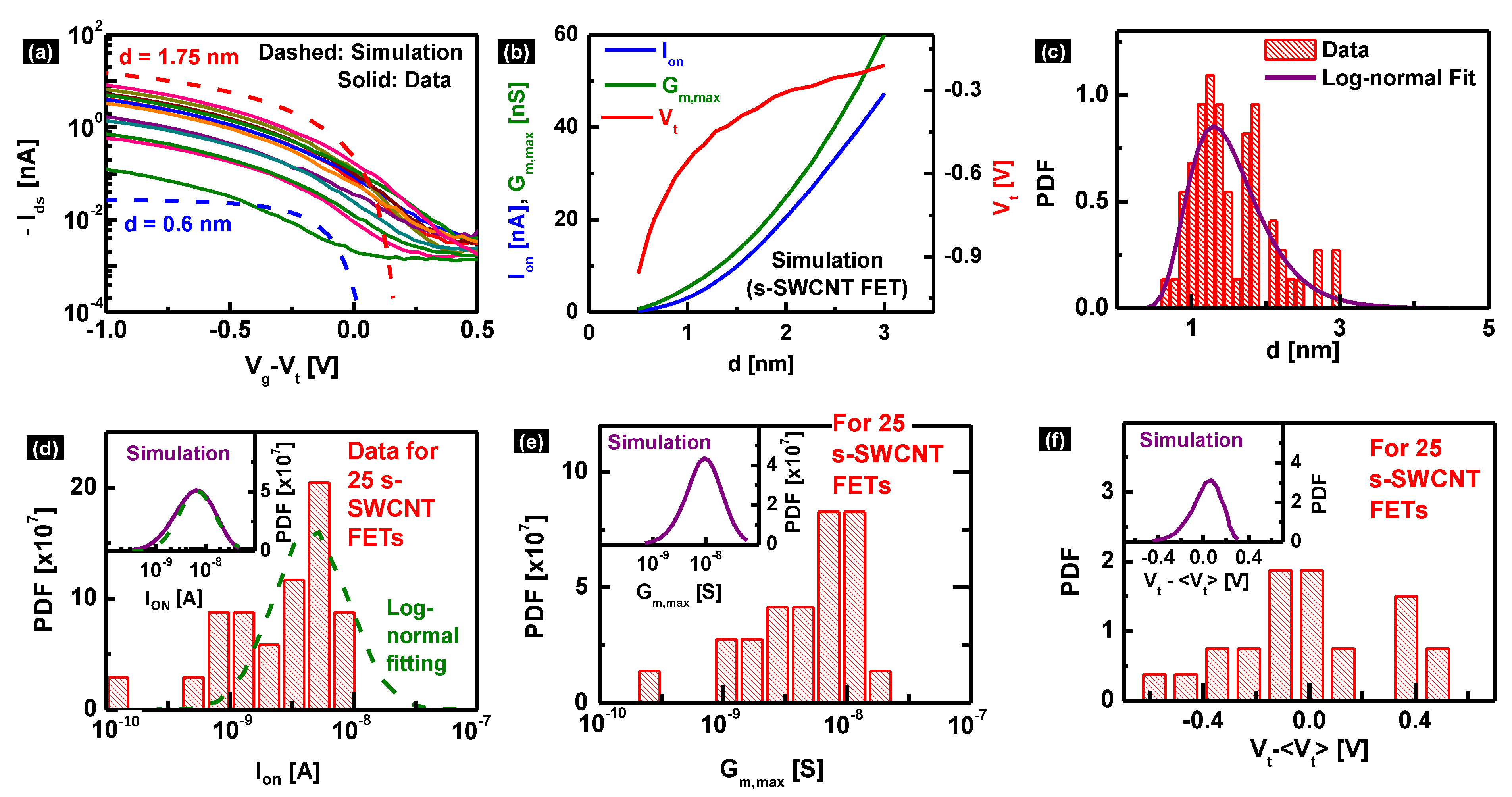
 (Figure 1a), aC-C = 0.142 nm is the C–C bond length, t ~ −3 eV is the C–C bonding energy. SWCNTs with n = m are called armchair nanotubes and always show metallic behavior, whereas SWCNTs with n ≠ m either show metallic behavior for mod (n − m)/3 = 0 or semiconducting behavior for mod (n − m)/3 = 1, 2. SWCNTs with m = 0 are called zigzag nanotubes and the rest with n ≠ m ≠ 0 are called chiral nanotubes.


