1. Introduction
Recent advancements in flexible electronics research will enable novel applications ranging from stylish flexible gadgets for real-time monitoring of health-related vital signs to novel biological applications such as electronic skin [
1,
2,
3,
4,
5,
6,
7,
8,
9,
10,
11]. Critical advances have been made in recent years that rely on organic materials as active elements because of their inherent flexibility. Mainstream approaches to capitalize on naturally flexible substrates like polymers can be categorized into (i) all-organic systems, where both devices (specifically active materials) and substrates are made up of organic materials [
12,
13,
14,
15,
16,
17,
18] or inkjet- and screen-printed in thin layers onto paper and organic substrates [
19,
20,
21,
22] and (ii) hybrid systems, where inorganic electronic devices are transferred onto an organic substrate using transfer printing and other transfer techniques [
23,
24,
25,
26,
27,
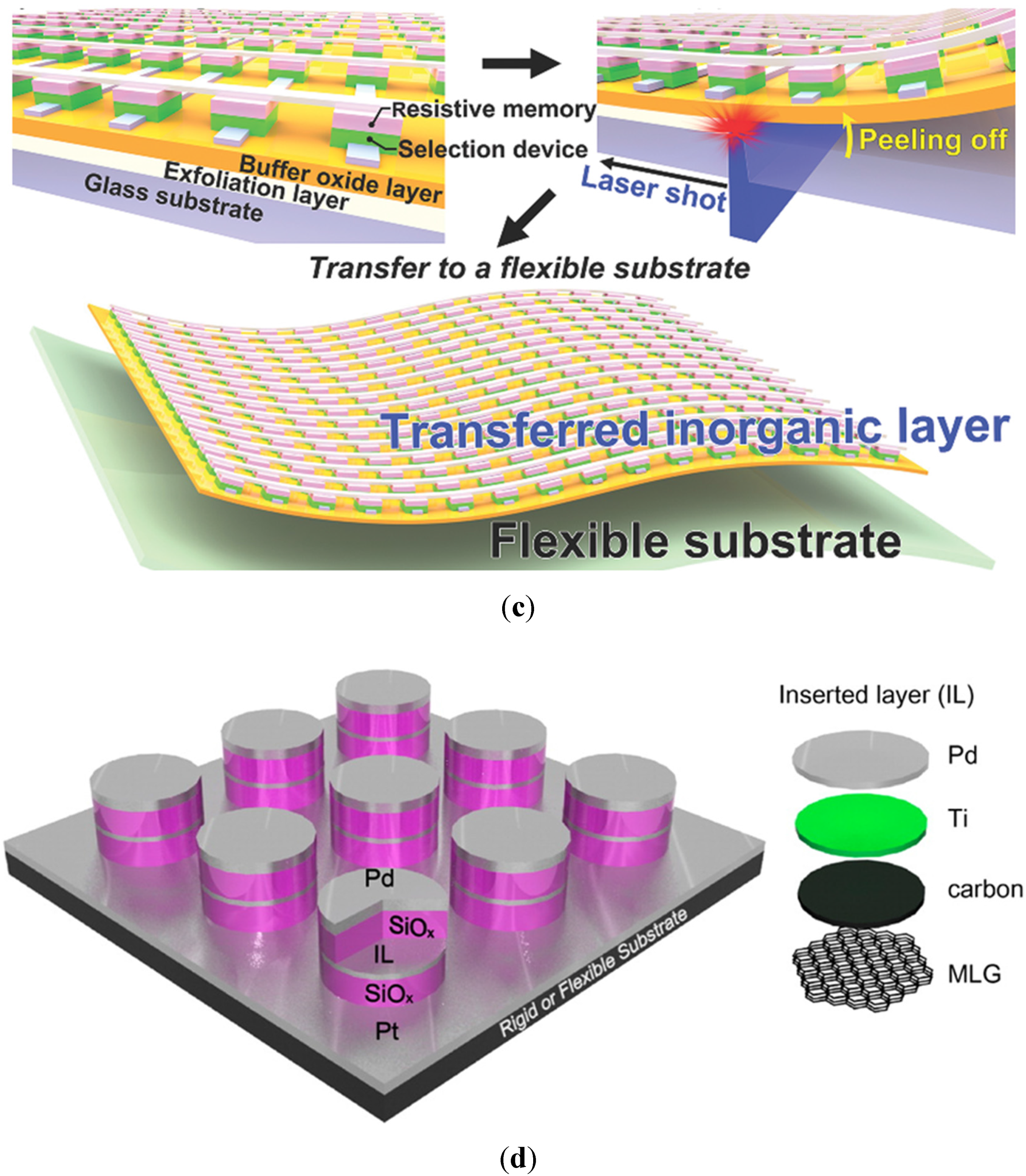
28,
29,
30,
31], laser lift-off transfer [
32], and low-temperature direct deposition of inorganic devices on plastic organic substrates [
33,
34,
35,
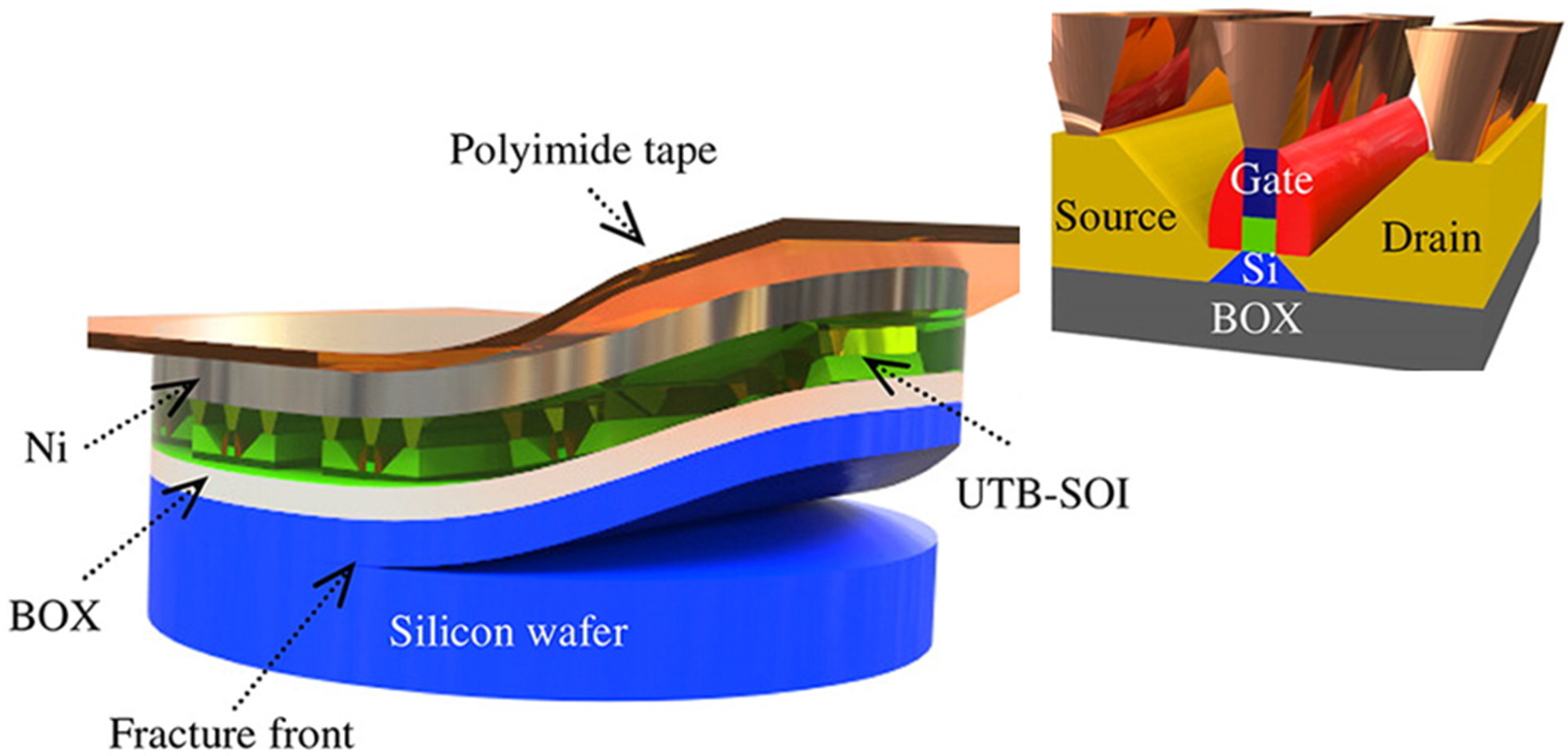
36]. Other approaches use silicon-on-insulator (SOI) substrates, and controlled spalling technology to peel-off thin semiconductor layers [
37,
38,
39]. In addition, a complementary transfer-free approach has recently been introduced, where thinning down the inorganic substrate through traditional, standard fabrication processes improves the flexibility of the substrate [
40,
41,
42,
43,
44,
45].
These approaches are all geared towards achieving fully flexible electronic systems. The three main components in any electronic system are (1) processing units; (2) the main memory; and (3) storage. Processing units perform logic operations through transistor logic, while the main memory performs temporary short-term storage (cache) with a quick access feature, also known as primary storage or random access memory (RAM), through access transistors and capacitors that store charges. Storage refers to the long-term retention of information, traditionally implemented using hard disks. However, at present, a shift towards other NVM types in a solid-state drive (SSD) format for supporting faster performance and higher integration densities within strict area constraints is taking place. Hence, the main electronic devices required to build an electronic system are transistors, capacitors, and NVM devices. Emerging NVM such as resistive random access memory (ReRAM), flash memory, phase change RAM (PCRAM), and ferroelectric random access memories (FeRAMs) have the benefits of fast switching, low-operation voltage, and ultra-large-scale-integration (ULSI) densities. These attractive qualities not only make them a favorable option for replacing magnetic hard disks but also for replacing quick access, volatile, dynamic RAM. This means that future electronic systems will require combinations of only two essential devices: transistors and NVM devices.
An objective assessment of the discussed mainstream and complementary approaches to flexible electronics must focus on their ability to provide high-performance, reliable NVM devices with ULSI density transistors. In this review, we present the mainstream NVM architectures and technologies with a special focus on most up-to-date techniques for producing flexible NVM devices.
Every memory cell consists of a gating device for access/select that is usually implemented using a transistor. Hence, memory arrays are where the largest number of transistors exist in an electronic system, a consequence of their ULSI density and low cost/bit ($/bit). Furthermore, with the continuous reduction in $/bit of NVMs and the higher switching speeds between memory states (‘0’ to ‘1’ or
vice versa) of emerging NVM technologies, replacing volatile random access memory and magnetic hard disks with faster SSDs made up of transistors and NVM structures becomes feasible. Here, the progress made over the past few years in three prominent types of flexible NVM technologies is discussed: (i) resistive; (ii) ferroelectric; (iii) phase change; and (iv) charge-trap** NVMs. In addition, the reliability aspects of the devices reported are discussed and an assessment for emerging technologies that provides useful insights towards their potential for commercialization is also provided.
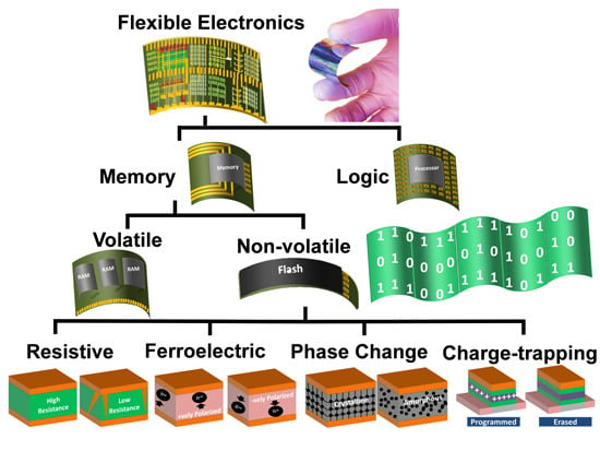
Figure 1 briefly positions the focus of this review in context with flexible electronics research.
Figure 1.
Chart highlighting the focus of the review.
Figure 1.
Chart highlighting the focus of the review.
In this review, our discussion is restricted to works that demonstrated an actual flexible version of flexible rewriteable NVMs between January 2010 and May 2015. However, there are many interesting works on flexible write-once-read-multiple (WORM) NVMs and other NVM devices that might be suitable for future applications in flexible electronics [
46,
47,
48,
49,
50,
51]. Furthermore, multiple interesting review papers are available on non-volatile memory technologies; however, the comprehensive scope of this review combining various flexing approaches, non-volatile memory and transistor technologies, arraying architectures with a special focus on flexibility, performance, reliability and monolithic integration ability has not been reported to date. For instance, Chung
et al. [
52], Makarov
et al. [
53], and Wang
et al. [
54] reviewed NVM devices but flexibility was not addressed. Naber
et al. [
55], Wang
et al. [
56], Liu
et al. [
57], and Chou
et al. [
58] reviewed only organic NVM. J.-S. Lee reviewed floating gate NVM devices [
59]. Lee and Chen [
60], Jeong
et al. [
61], Panda
et al. [
62], Lin
et al. [
63], Porro
et al. [
64], and Seok
et al. [
65] reviewed only resistive (ReRAM) NVM. Kim
et al. reviewed hybrid organic/inorganic nanocomposites materials for NVM [
66]. Liu
et al. [
67] and Mai
et al. [
68] reviewed only ferroelectric NVM and ferroelectric electronics. Kurosawa
et al. reviewed polyamide based memory [
69]. Han
et al. reviewed various flexible NVM technology but reliability issues, flexible access and logic transistors, and monolithic integration ability were not addressed [
70]. Acharyya
et al. reviewed the reliability of TiO
2 based ReRAM [
71], and Gale
et al. reviewed only TiO
2 based ReRAM [
72]. Therefore, this review is unique in its scope, providing a comprehensive perspective on the collective progress in the field of flexible electronics with a special focus on flexible nonvolatile memory technologies.
As of today variety of materials have been used to build NVM devices. For example, NMVs based on; (i) embedded 0-dimensional gold nanoparticles (NPs) [
73,
74,
75,
76,
77], black phosphorous quantum dots (QDs) [
78], and silicon QDs [
79]; (ii) 1-dimensional zinc oxide (ZnO) nanowires [
48], silicon (Si) nanowires [
80], and carbon nanotubes (CNTs) [
81,
82,
83]; and (iii) 2-dimensional graphene [
49,
84,
85], graphene oxide [
46,
86,
87,
88,
89,
90,
91], molybdenum disulfide (MoS
2) [
50,
92], zinc oxide (ZnO) [
48], and hydrated tungsten tri-oxide (WO
3.H
2O) nano-sheet [
29] have already been reported.
Although these and other similar reports have focused on discrete memory devices or cells, academic researchers and semiconductor industries have reported macroelectronics (large area electronics) focusing on mainly artificial skin [
93,
94,
95] and display technology where memory has not been an integrated built-in module. Sony reported a rollable organic light emitting diode (OLED) based display in 2010 [
96]. Samsung in the consumer electronics show (CES) 2011 and, later, LG and Nokia demonstrated a flexible display prototype [
97]. However, the futuristic vision of the IoT where everything is connected, communicating, and making real-time decisions with artificial intelligence, with the associated emerging markets of big data analysis and machine-to-machine (M2M) technologies, would require more than flexible displays. The steep increase in the number of sensors from few millions in 2007 to billions of devices in 2013 is expected to persist, reaching the trillion sensor devices mark by 2023 due to the impact of IoT [
98]. These sensors will be integrated in smart cards and RFIDs, vehicular technologies, buildings, infrastructures, healthcare, smart energy, factories, and supply chain management [
98,
99,
100], as well as on humans for improving regular day to day experience [
101]. To achieve such functionalities and fulfill the futuristic vision, IoT devices will require: (i) increased intra-node processing for real-time decision making; (ii) robustness to environmental variations (reliability); (iii) ultra-low power operation; (iv) ultra-high density integrated NVM and (v) smart antennas for wireless communications [
102,
103,
104,
105,
106]. In addition, IoT devices should be physically flexible to enable wider adaptation in wearable forms and conforming to curvilinear structures in various forms.
To this end, integrated device manufacturers (IDMs) have already demonstrated devices designed to meet the IoT requirements. In 2014, Aitken
et al. identified the 65 nm CMOS technology as the most suitable IoT chip process based on wafer cost and die area analysis [
107]. In 2015, Yamamoto
et al. demonstrated a novel gate stack in 65 nm CMOS technology for ultra-low leakage devices [
103], Ueki
et al. from Renesas Electronics Corporation developed a low power 2 Mb ReRAM macro in 90 nm CMOS technology [
108], Whatmough
et al. implemented a 0.6 volts transceiver in 65 nm CMOS technology [
109], and Yamauchi
et al. developed an embedded flash memory in vehicle control systems for IoT applications [
100]. Furthermore, Hitachi researchers have studied how to profit from IoT for 10 years and used big data analysis to introduce the wearable happiness meter to unravel the link between physical motion and happiness [
101]. Tanakamaru
et al. introduced privacy protection solid state storage (PP-SSS) for what they called, “the right to be forgotten,” where data is physically and automatically broken hardware-wise to co-op with anticipated security and privacy issues in the IoT era [
110]. These are all great milestone in providing useful insights of what the future holds with the IoT revolution.
Based on the existing progress and current status, it is evident that while IoT devices are required to attain physical flexibility, they still have to rely on CMOS technology while pushing for ultra-low power consumption, ultra-low leakage currents, improved reliability, and ultra large scale co-integration of NVMs, CPUs, and antennas. Flexible antennas have been studied decades and will not be discussed in this review [
111,
112,
113,
114,
115,
116]. As aforementioned, NVM modules require information storage elements and select access transistors; therefore, a NVM perspective of the flexible electronics arena provides a comprehensive overview of the basic elements needed for implementing all electronic systems, including systems suitable for IoT applications.
4. Flexible Field-Effect Transistors (FETs) for Logic and NVM Arrays
Today’s memories have the highest density and number of integrated transistors of all electronic systems. With the advent of big data, the introduction of cloud computing, and the extensive deployment of gigantic data centers, the demand for more storage space and high storage density is increasing. Therefore, it has become essential to survey state-of-the-art flexible transistors. We think it is important to note that these transistors are not to be confused with the transistors used in 1T memory architectures. Although both are field-effect transistors, their functionality is conceptually different. One function is to store/trap charges while the other is to act as an electronic switch. 1T transistors are evaluated based on their ability to store charges (retention), memory endurance, and their ability to shift the voltage threshold (memory window) properties, while access/select and logic transistors are evaluated with respect to their ability not to store charges, subthreshold slopes, drain-induced barrier lowering, and stability of the threshold voltage. In this section, we focus on the switching-type transistor that is used in circuit logic and as a select/access transistor for the storage structures in 1T1C, 1T1R, and 2T2C architectures.
Over the past half-decade, a large portion of the reported work on flexible transistors has focused on thin film transistors (TFTs), which are a subset of FETs. TFTs are common in display technology for controlling active matrix organic light emitting diode (AMOLED) pixels [
164]. Recently, however, they became popular for switching and logic computations due to their facile low-temperature fabrication on flexible substrates. The next subsections summarize the demonstrated flexible organic, hybrid, and inorganic FETs (mostly TFTs) over the past five years.
4.1. All-Organic Transistors
Table 2 highlights the demonstrated flexible all-organic transistors from 2010 up to May 2015. The best reported values are highlighted throughout for each performance metric; however, this does not mean that the most up-to-date technology is capable of being combined into one flexible all-organic structure with all the best performance because in most cases values are intertwined such that optimizing one value affects the others. For instance, increasing the thickness of the Ba
0.7Sr
0.3TiO
3 (BST) gate dielectric in an organic TFT can reduce the threshold voltage (V
th), increase the effective mobility (μ
eff); on the other hand, it can reduce the I
ON/I
OFF, and increase the subthreshold slope (SS) [
165]. In general, evidence suggests that the all-organic transistors suffer low mobilities (<10 cm
2/V.s), with the exception of graphene TFT, which achieves 340 cm
2/V.s [
166]. We would also like to highlight the excellent flexibility of the devices down to a bending radius of 100 μm [
167], and persistence up to 10,000 bending cycles [
168]. The minimum feature reported is in the order of tens of micrometers (with the exception of Min
et al. nanowires arrays, in 2013, achieving sub-micron dimensions [
120]), which is relatively large as is the operational voltage and SS in many of the demonstrated devices. The highest reported yield for all organic transistors is 66%, reported for ink-jet printed devices [
169].
Table 2.
Key works on flexible all-organic transistors from 2010 up to May 2015. Highlights showing the best values reported.
Table 2.
Key works on flexible all-organic transistors from 2010 up to May 2015. Highlights showing the best values reported.
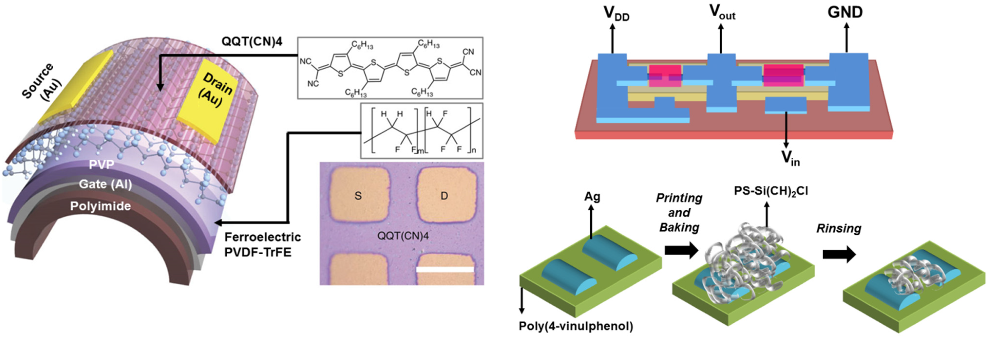
| Reference | [165] | [170] | [171] | [167] | [169] | [172] | [173] | [168] | [174] | [175] | [176] | [166] | [120] | [177] |
| Year | 2012 | 2012 | 2012 | 2010 | 2013 | 2013 | 2013 | 2014 | 2014 | 2015 | 2010 | 2014 | 2013 | 2015 |
| Structure | PEN/Ag gate BST dielectric/pentacene channel/Ag source and drain | PET/Al source and drain/C60 channel/Parylene-C dielectric/Al gate | Metal gate/Mylar/TIPS-pentacene/Metal source and drain | PI/Al gate/ hybrid (AlOx)-organic self-assembled monolayer (SAM) gate dielectric/Pentacene p-channel/Au source and drain | PET/ SWCNT/Ag source and drain/Barium titanate NP in PMMA ink dielectric/Ag gate | Au gate/Parylene dielectric/Au source and drain/TTC18-TTF channel | PI/gate electrode/Parylene dielectric/C8-BTBT channel/Au source and drain/Parylene/PI | PI/Al gate/c-PVP/c-PVP/Pentacene/ Au source and drain | PET/Ag source and drain/barium titanate -BTO-poly(methyl methacrylate) dielectric/Ag gate | PET/ITO gate/PVP dielectric/Pentacene channel/Au source and drain | PEN/Al gate/PI dielectric/QQT(CN)4/Cr-Au source and drain | PET/Ti-Au source and drain/Graphene/PMMA/Au gate | PAR/Au source and drain/P3HT:PEO-blend NW/ion-gel polyelectrolyte/Au gate | PEN/PVP/Ag gate/Parylene dielectric/Ag source and drain/DTBDT-C60 semiconductor |
| Approach | All organic | All organic | All organic | All organic | All organic (Ink-jet Printed) | All organic | All organic (Ink-jet Printing) | All Organic | All Organic (Screen Printing) | All Organic | All Organic | All Organic (Low Temperature Deposition + Graphene Transfer) | All organic | All organic |
| Dimensions (µm) | 100 × 2000 | 70 × 1800 | | 50 × 500 | 85 × 1250 | 20 × 5000 | length is 20 | 150 × 1500 | 105 × 1000 | 100 × 500 | 45 × 4000 | 10 to 20 length | 0.34 × 0.31 | 90 × 1100 |
| Mobility (cm2/VS) | 0.53–1.24 | 0.58 | 0.1 to 0.4 | 0.5 | 9 | 0.0043 | 0.15 | 0.56 | 7.67 | 0.45 | 0.1 to 0.006 | 340 | 9.7 | 1.9 |
| SS (mV/Dec) | 100–160 | 1250 | 5000 | 166 | | | ~3300 | 2300 | | 1000 to 1500 | | | 250 | 170 |
| Vth (V) | −1.11 to −1.18 | −0.1 | ~10 to 30 | ~−0.5 | 1.15 | 20 | ~10 | −0.82 | | | | | 0.5 | −0.16 |
| Operation Voltage (V) | 3 | | 10 to 40 | 3 | −10 to 10 | | 10 to −50 | −4 to 4 | <10 | 10 to −30 | 100 to −100 | −60 to 40 | 2 | 20 |
| min bending radius (mm) | 3 | 5.1 | 0.26 unencapsulated and 0.11 encapsulated in Parylene | 0.1 | 1 | 2 | 1 | 0.75 | 3 | 2 | 5 | 10 | | 6.25 |
| ION/IOFF | 104 | 105 | 5 × 10³ | 1.5 × 10³ | 105 | 500 | 5 × 10⁴ | 105 | 104 to 105 | | | | 105 | 108 |
| Yield | | | | | 66% | | | | | | | | | |
| Bending cycles | | | | | | | | 104 | | | | | | |
Table 3.
Summary of demonstrated hybrid flexible devices over the past half-decade.
Table 3.
Summary of demonstrated hybrid flexible devices over the past half-decade.
| Reference | [178] | [179] | [180] | [181] | [182] | [183] | [184] | [28] | [185] | [186] | [187] | [188] | [189] | [190] | [191] | [192] | [193] |
| Year | 2013 | 2014 | 2013 | 2014 | 2014 | 2014 | 2014 | 2014 | 2011 | 2012 | 2013 | 2014 | 2014 | 2015 | 2015 | 2015 | 2013 |
| Structure | Parylene/Au gate/Parylene dielectric/pentacene channel/Au source and drain | Au source and drain/ (P(NDI2OD)T2 or N2200) n-type or (pBTTT) p-type/PMMA dielectric/Au gate | PVA/PMMA/Au source and drain/MoS2/Al2O3/Cu gate | PEN/Buffer/Al gate/Al2O3/a-IGZO/Mo-Al-Mo source and drain/PR protection | PI/Ni gate/PVP/Al2O3/a-IGZO/Ni source and drain | PDMS/CuPc NW/metal source and drain/Si3N4/Metal Gate | PI/Cu and MoTi Source and drain/organic semiconductor OSC active/organic gate insulator OGI/Cu gate | PI/ Inorganic Si FinFET | PI/IGZO TFT/PI | PI/SiO2-SiNx-SiO2-SiNx-SiO2/Mo gate/ Hybrid organic-inorganic S-ALO/Au Source and Drain/TIPS PEN:PS Channel | PI/IGZO TFT | Kapton Tape/IZO TFT/ | CPI/IGZO TFT | PI/ZnO TFT | PI/PVP/Al gate/PVP/ZrO2:B/In2O3/Al | PVP/AlOx /aZITO/AryLite | Kapton/PI/Ti/Pd/Al2O3 or HfO2/MOS2/Ti/Au |
| Approach | Hybrid (Transfer) | Hybrid (Transfer) | Hybrid (Transfer) | Hybrid (Deposition at Low Temperature) | Hybrid (Deposition at Low Temperature) | Hybrid (Transfer) | Hybrid (Transfer) | Hybrid (Transfer) | Hybrid (Transfer + encapsulation) | Hybrid (Detachment from Glass Substrate) | Hybrid (Deposition at Low Temperature) | Hybrid (Deposition at Low Temperature) | Hybrid (Deposition at Low Temperature) | Hybrid (Deposition at Low Temperature + Strip** off Si | Hybrid (Deposition at Low Temperature) | Hybrid (Deposition at Low Temperature) | Hybrid (Deposition at Low temperature) |
| Dimensions (µm) | 2 to 10 gate length | 20 × 1000 | 4.3 × 10 | 100 × 100 | 60 × 800 | 10 × 200 | 6 × (14–−160) | 0.25 × 3.6 | 115 × 280 | 4 × 20 to 6000 | 6 × 50 | 50 × 1000 | L 20 × W 10 | 20 × 200 | | 50 × 1000 | 1 × 3 |
| Mobility (cm2/VS) | 0.0013 to 0.00022 | 0.1 to 0.3 | 19 | 11.2 | 5.3 to 8.39 | 2 | 0.34 | 141.53 (N) to 13.22 (P) | 13.7 | 0.61 | 18 | 6 to 11.2 | 12.7 | 12 | 0.42 | 10.9 | 30 |
| SS (mV/Dec) | ~5000 | | 250 | 270 | 520 to 960 | | | 80 (N) to 70 (P) | | 200 | | 2000 to 4600 | 160 | | | | 82 |
| Vth (V) | −4 to 9.5 | | −2.12 | 0.5 | 7.03 to 9.8 | | | 0.345 (N) to 0.713 (P) | 0.154 | −0.27 | 0.9 | 18.8 to 31.3 | −1.7 | | 8.07 | 0.7 | −2 |
| Operation Voltage (V) | −32 | 20 to 50 | −5 to 2 | 10 to 10 | 20 to −10 | −10 | 30 to −30 | −1.5 to 1.5 | 5 | 0.5 to 2 | 5 | | −20 to 20 | 8 | −40 to 40 | 3 | 3 |
| Switching time (ms) | | | | | | | | | | | | | <0.8 × 10⁻³ | | | | |
| min bending radius (mm) | 0.4 to 0.8 | 1 | 5 | 10 | 10 | 3 | 4 | 5 | 0.125 | 2 | 5 | 10 | 2 | 3.3 | 5 | 10 | 1 |
| ION/IOFF | 104 | 105 | 106 | 109 | 1.4 × 10⁵ to 3.5 × 10⁶ | 104 | 107 | 104.6 (N) to 104.78 (P) | | 107 | | 3.8 × 10⁴ to 1.5 × 10⁶ | | 108 | 3.69 × 10⁵ | 105 | 107 |
| Yield | | 90% | | | | | | 60% | | | | | | | | | |
| Bending cycles | | | 10 | 106 | 105 | 450 | 105 | | | 5000 | | 1000 | 1000 | 5 × 10⁴ | 104 | 100 | |
4.2. Hybrid Transistors
Table 3 highlights the demonstrated hybrid flexible devices. Evidently, device flexibility was lower than for those with all-organic materials such that more than 80% of the devices had a minimum bending radius of ~2 mm or above. This result is expected because the process is more complex and involves inorganic and inflexible materials. Nevertheless, an exceptional dynamic stress stability of up to one million bending cycles was demonstrated for a 10-mm bending radius [
181]. The hybrid approach showed mild improvements over the all-organic transistors with mobility values often above the 10 cm
2/V.s threshold; although, one reached 141 cm
2/V.s [
28] with lower SS and operating voltages. Also minimum features of a few microns were demonstrated in many cases, an order of magnitude improvement from the tens of microns features for all organic transistors, with a few exceptions of submicron-scale gate length devices [
28,
37,
74]. Also an order of magnitude improvement in the best I
ON/I
OFF ratio [
181], and 90% yield have been reported [
179].
4.3. Inorganic Transistors on Flexible Silicon
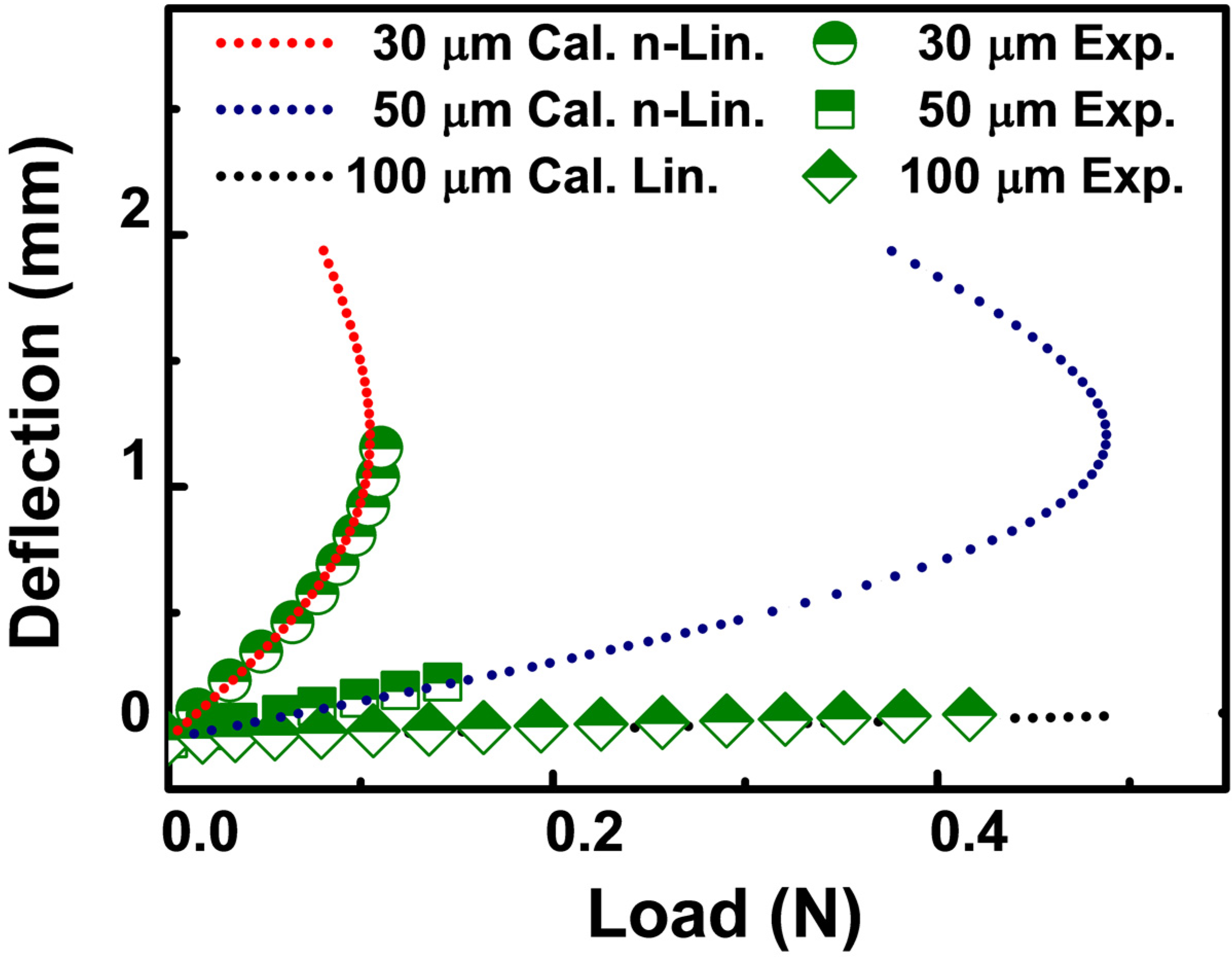
Table 4 highlights works on flexible inorganic FETs. Two types of inorganic flexible CMOS transistors on Si have been reported: traditional planar metal oxide semiconductor FET (MOSFET) [
125,
194,
195] and 3-dimentional out-of-plane architectural Fin-FET [
45]. The electrical and mechanical reliability aspects of the flexed transistor gate stacks, made up of a high-dielectric constant (κ); ALD Al
2O
3, has also been reported and shows a lifetime degradation from electrical stress when the stacks are flexed [
196]. The degradation is attributed to increased interfacial charges, leading to a 20% decrease in the safe operational voltage, which would satisfy the ten-year projected lifetime industry standard. A further mechanical reliability assessment was done by observing the effect of mechanical stress on the breakdown voltages of the devices [
197]. The results showed that (i) the breakdown voltage increased with more severe bending (lower bending radius/higher strain and stress); (ii) constant mechanical stress might have the same effect as constant electrical stress, and, most notably; (iii) the most severe degradation occurred in devices under dynamically varying mechanical stress (limited number of bending cycles ~100). Otherwise, functionality was reported to pass 200 bending cycles for planar MOSFETs [
195], as reliability studies impose harder stress conditions than a device would normally experience for accelerated tests. The minimum bending radii increased considerably to 0.5 mm [
45], while the SS, operation voltages, and most importantly, minimum features (tens of the nanometer scale [
195]) scaled down. Peak reported mobility of 252 cm
2/V.s was reported by Zhai
et al., in 2012 [
125].
To conclude, the CMOS based flexible transistors are promising candidates for future flexible IoT devices because of their monolithic integration ability, superior electronic properties inherent from bulk form, and almost uncompromised reliability. However, the assessed degradation in performance and safe operation voltages should be accounted for when designing flexible electronic systems utilizing the flexible devices. Another important milestone to achieve fully flexible electronic systems and devices for IoT applications is demonstrating suitable flexible NVMs that can be co-integrated with the flexible transistors for memory storage, without compromising integration density, system speed, and reliability.
Table 4.
Works on flexible inorganic field effect transistors (FETs) between January 2010 and May 2015.
Table 4.
Works on flexible inorganic field effect transistors (FETs) between January 2010 and May 2015.
| Reference | [194] | [45] | [125] | [195] |
| Year | 2013 | 2014 | 2012 | 2012 |
| Structure | Si/NiSi/Al source and drain/Al2O3 dielectric/TaN-Al gate | Inorganic FinFETs on Thinned Si | Inorganic Planar MOSFETs on Exfoliated Si | Inorganic Planar MOSFETs on Thinned Si |
| Approach | Inorganic (Etch-protect-Release) | Inorganic (Soft Back Etch) | Inorganic (Exfoliation) | Inorganic (Spalling) |
| Dimensions (μm) | 8 length × 5 width | 0.25 (P) to 1 (N) × 3.6 | 0.15 to 1 length | 0.03 length |
| Mobility (cm2/VS) | 43 | 102 (P) | 252 (N) to 51 (P) | |
| SS (mV/Dec) | 80 | 150 (N) to 63 (P) | 81 (P) to 72 (N) | |
| Vth (V) | −0.44 | 0.36 (N) to −0.556 (P) | | 0.25 |
| Operation Voltage (V) | 1 to −2 | −1.25 to 1.25 | −1 to 1 | 0.6 |
| Switching time (ms) | | | | <16 × 109 |
| min bending radius (mm) | | 0.5 | | 6.3 |
| ION/IOFF | 104 | 105 | 106 (P) | 105 |
| Yield | | 75% | | |
| Bending cycles | 5 | | | 200 |
6. Conclusions and Future Prospects
Exciting progress has been made in flexible electronics research over the past few decades. OLED flexible screens are already available in the market, and numerous novel biomedical and wearable applications using flexible electronics have been proposed. At this stage, expectations for silicon-based electronics are high and the status quo is for high performance, fast, low power, compact, and reliable aspects, some of which might not cross the chasm to the flexible arena. This is the core value for which the research field of transfer-free inorganic silicon-based flexible electronics is created. However, this approach is relatively new compared to the ongoing research on flexible organic electronics, where organic materials are used as substrates or device material.
In this review, we have presented a brief overview of flexible electronics research, focusing on NVM components. We listed the mainstream NVM architectures and technologies with a special focus on flexible devices and provided benchmarking tables for transistors and storage devices derived from the three main approaches: (1) all organic; (2) hybrid; and (3) inorganic.
Future prospects indicate that a number of challenges will have to be overcome before flexible ReRAM, FeRAM, PCRAM, MRAM, and flash will be primed for commercialization. Flexible FeRAM has an edge because of its rigid current form that is used as an embedded NVM in microprocessors. Flash has the highest potential owing to the maturity of the technology in the rigid state; furthermore, the transfer of this technology and progress to the flexible arena will definitely speed up the introduction of commercial flexible flash NVM for various applications. On the other hand, ReRAM, PCRAM, and MRAM are still emerging technologies, even in their bulk rigid form. The potential for extreme scaling, fast speeds, and low-power operation of NVMs is attracting the attention of both researchers and industry such that they might catch up with competing mature technology in the flexible arena earlier than expected.
Table 9.
Summary of the key works on flexible Flash memory over the past five years.
Table 9.
Summary of the key works on flexible Flash memory over the past five years.
| Reference | [260] | [82] | [80] | [76] | [77] | [262] | [74] | [85] | [73] | [261] |
| Year | 2012 | 2011 | 2012 | 2014 | 2011 | 2012 | 2010 | 2012 | 2013 | 2015 |
| Memory Type | Flash + Nano Particles (1T) | Flash (1T) | Flash (1T) | Flash (1T) | Flash (1T) | Flash (1T) | Flash (1T) | Flash (1T) | Flash (1T) | Flash (1T) |
| Flexible Final Structure | PET/Ag gate electrode/Al2O3/PMMA with Au NP composite/Pentacene/Au source and drain electrodes | PET/graphene gate electrode/Al2O3/CNT channel/graphene for source and drain electrodes | PES/Si NW/Al2O3/Pt-NP//Al2O3/Al source, drain, and gate | PET/ P(NDI2OD-T2) Channel/ Au source and drain/PVA tunneling dielectric/ Au-NP/ P(VDF−TrFE−CFE) blocking dielectric/ Al gate | PES/ITO gate/PVP blocking/APTES-Au-NP/PVP tunneling/MoO3 buffer/ Pentacene channel/ITO source and drain | PES/Al source and drain/ZnOPDA/AlOx-SAOLs/Zno:Cu/AlOx-SAOLs/Pentacene/ Al gate | PES/Ti-Au gate/ PVP blocking/ APTES-Au NP storage/PVP tunneling/ Pentacene channel/ Au source and drain | PEN/graphene channel/Al2O3/HfOx/Al2O3/ ITO | PET/ITO gate/Al2O3/Au NP charge trap**/Al2O3/PDPP-TBT/Au source and drain | PDMS/PI/Au/Al2O3-SiO2/SWCNT/Au |
| Approach | All organic | All organic | Hybrid (Transfer) | All organic | All organic | Hybrid (Low Temperature Deposition) | All organic | Hybrid (Deposition at Low Temperature) | All organic | Hybrid (Transfer) |
| Operating Voltage (V) | −5 to +5 | −10 to +10 | −10 to +10 | −6 to +6 | −90 to +90 | −15 to +15 | −90 to +90 | −21 to +23 | −40 to +40 | −25 to +25 |
| Form Factor (F2) | 10 | -- | -- | 20 | 10 | 2 | 10 | 6.67 | 20 | 11 |
| Memory Window | 2.1 | 10 | 1.85 | 2 | 15 | 14.1 | 9.7 | 8.6 | 7.5 | 13.2 |
| Speed (ns) | -- | 100 | 107 | 2 × 10⁹ | 1 × 10⁹ | 1 × 10⁸ | 1 × 10⁹ | hypothesized ~14 ns read time and 20 μs/20 ms write/erase time | 10 × 107 | 105 |
| Endurance (cycles) | 1000 | 500 | 104 | 105 | -- | -- | 700 | -- | 1000 | 104 |
| Retention (s) | 105 | 1000 | 104 | 105 | 105 | 1000 | 105 | 30% after 10 years | 106 | 104 |
| Operating temperature (°C) | 100 | 25 | 25 | 25 | 85 | 25 | 25 | degrades at 85 | 25 | 25 |
| Bending Radius (mm) | 10 | 8 | 16 | 9 | 20 | -- | 20 | 5 | 10 | 5 |
| Bending Cycles | 1000 | 1000 | 1000 | 100 | 2000 | -- | 1000 | 10 | 1000 | 1000 |
| Yield | -- | -- | -- | -- | -- | -- | -- | -- | -- | -- |
| Cell Dimensions (μm) | 50 × 500 channel | -- | 2 channel length | 100 × 2000 channel | 100 × 1000 channel | 50 × 100 channel | 100 × 1000 channel | 30 × 4.5 channel | 50 × 1000 channel | 18 × 200 |
These novel flexible NVM technologies along with the required flexible transistors for array gating and data processing are enabling technologies for the foreseen future where a galactic network of connected devices can autonomously detect, collect, and process surrounding information to make real time decisions fulfilling the IoT futuristic vision. The NVMs will store instructions and data in both power-on and power off states consuming minimal power. Furthermore, to meet the ultra-low power requirements for IoT devices when the collected information does not need real time processing, integrating ultra-high density NVMs will help store large amount of information to be analyzed when the device is externally charging, instead of sending data continuously through an antenna and consuming extra power. This is useful when collecting activity level throughout the day, similar to the study conducted by Hitachi that provided a link between variability of motion and happiness. NVMs will also have to cope with ultra-large scale integration to be able to store the huge amounts of information for big data analysis, in compact ultra-mobile devices, that can be preferably monolithically integrated in state-of-the-art CMOS technologies to expedite its introduction in the consumer electronics market. However, the status quo of flexible NVMs shows that there is still a gap between current bulk devices’ properties and their flexible counterparts. Hence, flexible NVMs and flexible electronic systems are still hindered from invading the consumer electronics market and still provide less attractive alternative to replacing bulk devices for future IoT applications. The core challenge is to either invent new technologies that can rival CMOS integration ability and standard processes at a reasonable cost, or to embrace CMOS technology in making flexible devices while obtaining flexibility as an extra feature without affecting critical performance metrics of the devices.


