Article

A 6-Bit Ku Band Digital Step Attenuator with Low Phase Variation in 0.13-μm SiGe BiCMOS

1
Institute of RF-& OE-ICs, Southeast University, Nan**g 210096, China
2
Engineering Research Center of RF-ICs and RF-Systems, Ministry of Education, Southeast University, Nan**g 210096, China
*
Author to whom correspondence should be addressed.
Electronics 2019, 8(10), 1149; https://doi.org/10.3390/electronics8101149
Submission received: 19 September 2019 / Revised: 7 October 2019 / Accepted: 9 October 2019 / Published: 11 October 2019
(This article belongs to the Special Issue Microwave Integrated Circuits Design and Application)

Abstract

:
A 6-bit Ku band digital step attenuator with low phase variation is presented in this paper. The attenuator is designed with 0.13-μm SiGe BiCMOS process technology using triple well isolation N-Metal-Oxide-Semiconductor (TWNMOS) and through-silicon-via (TSV). TWNMOS is mainly used to improve the performance of switches and reduce the insertion loss (IL). TSV is utilized to provide approximately ideal global current ground plane with low impedance for the attenuator. In addition, substrate floating technique and new capacitance compensation technique are adopted in the attenuator to improve the linearity and decrease the phase variation. The measured results show that the attenuator IL is 6.99–9.33 dB; the maximum relative attenuation is 31.87–30.31 dB with 0.5-dB step (64 states), the root mean square (RMS) for the amplitude error is 0.58–0.36 dB and the phase error RMS is 2.06–3.46° in the 12–17 GHz frequency range. The total chip area is 1 × 0.9 mm2.

Graphical Abstract

1. Introduction

The attenuator is one of the key components of modern communications. It is widely used in the transmitter/receiver (T/R) module of phased array radar system [1,2], and its main function is to achieve amplitude control. Compared with the X-type attenuator [3] and variable gain amplifier (VGA) [4,5], the passive digital step attenuator has the advantages of low power consumption, high linearity, wide frequency band and low temperature drift. Therefore, the design of attenuator with high resolution, large attenuation, low IL and low phase variation has great value, and very broad application prospects.
A variety of passive attenuator circuits have been designed in [6,7,8,9,10,11,12,13,14,15,16,17,18,19,20,21,22,23,24]. There are three most-used topologies in the passive attenuators: Switched path attenuators [6,7,8,9], distributed attenuators [10,11] and switched T/Pi attenuators [12,13,14,15,16,17,18,19,20,21,22,23,24]. Switched path attenuators topology use single-pole-double-throw (SPDT) switches to control the signal between reference thru line path and the resistive attenuation network path. This topology exhibits low phase variation, but has high insertion loss and large chip area, so it is not suitable for multi-bit CMOS digital step attenuator. Transistors as varistors and the half/quarter-wavelength of the transmission lines (TLs) together constitute the distributed attenuators topology. Due to the relative attenuation signal paths across the transmission lines have no series switches, this topology has the advantage of low IL. Meanwhile, the use of the TLs greatly increases the chip area. Switched T/Pi attenuators topology is composed by the resistor attenuation network and series shunt single-pole-single-throw (SPST) switches. Its chip area is very compact and suitable for multi-bit integration.
In order to meet the design requirements of phased array system for attenuators with high resolution, large attenuation, low IL and low phase change, this paper proposed a 6-bit CMOS digital step attenuator using switched T/Pi topology. The switches are designed and optimized by TWNMOS and through-silicon-via (TSV), in order to improve the performance and reduce the IL of the switches. Moreover, the attenuator adopted substrate floating and new capacitance compensation technology, which improved linearity and reduced the phase variation.

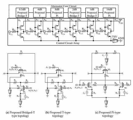
2. Proposed Circuit Design and Analysis

The switch is one of the key building blocks in the digital step attenuator [25,26]. In this paper, the triple well isolation NMOS is adopted in the switch shown in Figure 1a. Figure 1b,c illustrate the simplified equivalent circuits for on-state and off-state of the switch. As shown in Figure 1, the on-resistance Rch and parasitic resistance at source and drain terminals of NMOS switch will contribute to the insertion loss in the signal path. The parasitic capacitors CGS, CGD, CSB and CDB will contribute to the off-capacitance Coff of NMOS switch and act as a leak path from input to output at the off-state. A large resistor RG (10 kΩ) is used to prevent the RF signal from leaking through the bias line. Body floating technique is used to improve power handling of the switch by reducing the signal loss through source/drain-to-body junctions. To implement this technique, a large resistor RB (10 kΩ) is added to the body terminal of the switch to enhance the linearity and insertion loss performance. Meanwhile, TSV is utilized to provide approximately ideal global current ground plane with low impedance for the attenuator.
Inductive and capacitive correction structure digital step attenuator is adopted in [18] to achieve low phase variations. Although the inductance correction structure can achieve low IL, it occupies a large chip area. Capacitance correction structure has the advantages of lower phase variation and better agreement with simulation results in the broadband frequency range, but it has larger IL than inductance correction structure. In order to solve the contradiction between large IL and low phase variation of capacitance correction structure, especially large attenuation units, such as 8 dB and 16 dB attenuation cells. A new capacitance compensation technique is proposed in this paper. The topology of the proposed capacitance compensation correction network attenuation cell circuits in the digital step attenuator is shown in Figure 2.
In the proposed circuit structure, a parallel capacitor CP is added to the shunt branch of the traditional T-type attenuator in Figure 2a. Ron is the on-resistance, and Coff is the off-capacitance of the transistor. When the switch M1 is on, and M2 is off, the attenuator works in the reference state. The signal passes through the series path, as shown in Figure 2b. When the switch M1 is off, and M2 is on, it works in the attenuation state. The signal flows from the shunt attenuation branch to the ground, as shown in Figure 2c. Parallel capacitor CP is introduced as a phase correction device in the attenuation branch. Therefore, the correction network will affect the performance of the attenuation state. In order to facilitate the theoretical analysis, the TSV and body series parasitic inductance are neglected. The simplified equivalent circuit of the phase correction branch is as shown in Figure 2d, and the transmission phase of the network can be derived from the transmission (ABCD) matrix of the attenuation state; the equation of transmission phase θ can be deduced as follows (see Appendix A for detailed derivation):
θ = tan 1 C p R p 2 ( Z 0 + R s ) ( R p + R o n ) ( 2 R p + 2 R o n + Z 0 + R s ) / ω + 2 R p 4 C p 2 ω + R p 2 C p ( Z 0 + R s ) ,
where ω is the operating angular frequency. Z0 is the characteristic impedance. For simplicity, all parameters in the equation are treated as the constant except the operating angular frequency ω.
The theoretical mathematical analysis image of function θ can be drawn using MATLAB in Figure 3a. The slope of θ changes from negative to positive value at the broadband angular frequency range. When the slope is zero, there exists a critical frequency f (f = ω/2π), which can be used to correct the transmission phase error.
Figure 3b shows the practical simulation results in 0.13 μm SiGe BiCMOS process of the transmission phase of the phase correction branch in Figure 2d. The transmission phase varies with parallel Cp value (swept from 60 fF to 180 fF) at the broadband frequency range. Figure 3a,b possess a similar variation tendency, which verifies the theoretical analysis results in Equation (1).
Figure 4a shows the proposed T-type attenuator topology transmission phases of reference and attenuation states are simulated with various parallel capacitor Cp value. The phases of attenuation states have the same variation trend as those of the phase correction branch in Figure 3b.
It is obvious that the capacitance variation influences the attenuation state significantly, whereas, it has less effect on the reference state. By adjusting the capacitance Cp value, we can control the transmission phase of reference and attenuation states to intersect at different frequencies to produce zero phase difference. The low phase difference in a specific frequency band can be achieved by choosing the appropriate capacitance Cp value, as shown in Figure 4b.
Figure 5a shows the simulation attenuation results with traditional T-type and proposed Cp T-type topology in 4 dB attenuation cell. The simulation phase difference results with traditional T-type and proposed Cp T-type topology in 4 dB attenuation cell is illustrated in Figure 5b. With Cp compensation circuit structure, Flatness of the phase difference is better in a wide bandwidth range.
Meanwhile, in order to study the influence of TSV on phase difference, parasitic parameters of TSV with different sizes can be obtained by the electromagnetic field (EM) simulation. Table 1 shows parasitic inductance and resistance of TSV with different sizes.
TSV is utilized to provide approximately ideal global current ground plane with low impedance for the attenuator. Take the proposed Cp T-type topology in 4 dB attenuation cell as an example, the TSV connected to the switch body terminal mainly provides on-chip grounding of the substrate, and its effect on the phase variation of the attenuator can be neglected. The TSV connected to capacitance compensation correction branch of the attenuation cell also provides on-chip grounding. The parallel capacitor Cp grounding terminal of the capacitance compensation correction branch in attenuation cell is not ideal, which results in an additional phase variation of the attenuator circuit. Although the effect of TSV on attenuator performance is small, it cannot be ignored. The simulation phase difference results with TSV size variation in proposed Cp T-type topology in 4 dB attenuation cell is illustrated in Figure 6. In microwave and millimeter wave bands, TSV will inevitably introduce parasitic inductance and resistance. The parasitic parameters are related to their size (i.e., the number of rows and columns vias). The larger the size, the smaller the parasitic inductance and resistance, but the bigger size will occupy a large area of the layout, so a compromise should be considered. After careful consideration, the TSV size of 2 × 5 was selected in this design.
The proposed capacitance compensation correction network and switch are also applicable to the Pi and bridge-T type attenuation cells. They have the same operation principle to realize low phase difference as the proposed T-type attenuator topology.
Traditional capacitance Cc and Cp compensation correction networks are widely used in the digital control step attenuator circuit [18,20,21], but there are large insertion losses, especially in large 8 and 16 dB attenuation units. In order to solve this problem, a parallel capacitor Cp is added to the attenuation shunt branch in 8 and 16 dB attenuation cells. Take 16 dB attenuation unit as an example: Figure 7a shows the simulation IL results with traditional Cc and proposed Cc + Cp compensation in 16 dB attenuation cell. The IL decreases obviously with the increase of frequency in the proposed Cc + Cp compensation structure. The simulated attenuation, phase difference results with traditional Cc and proposed Cc + Cp compensation in 16 dB attenuation cell is illustrated in Figure 7b. With Cc + Cp compensation circuit structure, the attenuation and phase difference change more smoothly in a wide frequency band.
Through the above theoretical and simulation analysis, in the proposed 6-bit digital control step attenuator circuit, 0.5 db, 1 db, 2 dB and 4 dB attenuation units adopt the proposed parallel capacitor Cp compensation method, which reduces the additional phase shift of attenuation. In the large attenuation unit (8 db, 16 db), we combine the traditional capacitance compensation method with the proposed parallel capacitance Cp compensation method, which reduces the problems of excessive insertion loss and large phase shift fluctuation range in the traditional capacitance compensation method.
The utilized attenuation cell topology in 6-bit CMOS digital control step attenuator is shown in Figure 8. 0.5 dB, 1 dB and 2 dB attenuation cells are configured with switched bridge-T type in Figure 8a. 4dB attenuation cell is configured with switched T-type in Figure 8b. The switched Pi-type topology in Figure 8c is suitable for large attenuation cells, such as 8 and 16 dB cells. The block diagram of the proposed 6-bit digital control step attenuator is shown in Figure 9.
The component values of each attenuator unit are summarized in Table 2. The 6-bit CMOS digital control step attenuator circuit is optimized in terms of linearity, loading effect and power processing ability. Finally, the bit ordering 0.5-4-8-2-1-16 dB sequence is adopted in this paper. The proposed attenuator is controlled by the 6-bit digital signal control circuit array, Vc1, Vc2, Vc3, Vc4, Vc5, Vc6, which are used to control 0.5 dB, 1 dB, 2 dB, 4 dB, 8 dB, 16 dB attenuation modules, respectively. The layout of series/parallel resistors are the key components in the attenuator design; and the resistance values need to be carefully selected. In particular, small resistance values are realized by parallel connection of large resistance to reduce the influence of process variation effects. The power consumption of the attenuator is extremely low, which is contributed by the dynamic power consumption of inverters in each attenuation module.
The full chip electromagnetic (EM) simulation of the proposed 6-bit digital control step attenuator except resistors, capacitors and NMOS switch transistors components is realized in ADS Momentum in order to further ensure the performance. The transmission RF lines between the circuits of each attenuation cell are used to connect each module, which improves the matching performance and adjusts the transmission phase characteristics. Both input and output impedances of the proposed attenuator are matched to 50 Ω.

3. Measurement Results

The proposed 6-bit digital control step attenuator has been designed and fabricated in 0.13-μm SiGe BiCMOS technology. The die photograph of the proposed 6-bit digital control step attenuator is depicted in Figure 10. The total chip size is 1 × 0.9 mm2. All the DC Pads are bond wired to a PCB for chip testing, and the chip is probed with Cascade’s 100 μm ground-signal-ground (GSG) probes at the input and output ports. The power consumption of the proposed attenuator is extremely low and negligible.
The input return loss (RL) is >13 dB in Figure 11a and the output return loss is >14.1 dB in Figure 11b at 10–18 GHz for the 64 states. Figure 12 shows the measured insertion loss (of the reference state) is 6.99–9.33 dB and IP−1dB (of the reference state) is 13.6–16.2 dBm at 12–17 GHz. The maximum attenuation relative to that of the reference state is 31.87–30.31 dB with 0.5-dB step (64 states) at 12–17 GHz in Figure 13. The measured results show that the root mean square (RMS) for the amplitude error is 0.58–0.36 dB and the RMS phase error is 2.06–3.46° in the 12–17 GHz frequency range for the 64 states in Figure 14. The RMS for the amplitude error can be defined as:
A R M S = 1 N i = 1 N ( A m _ i A t h e o _ i ) 2 ( d B ) ,
where ARMS is the attenuation RMS amplitude error, I is the attenuation state index, N is 64, Am_i is the measured attenuation relative to the reference in a given state, and Atheo_i is the theoretical attenuation in a given state. The RMS phase error for the attenuation is calculated using the equation defined as follows:
θ R M S = 1 M i = 1 M ( θ m _ i θ r e f _ m ) 2 ( d e g ) ,
where θRMS is the attenuation RMS phase error, i is the attenuation state index, M is 64, θm_i is the measured attenuation relative phase in a given state, and θref_m is the measured attenuation relative phase in the reference state.

4. Comparison with Relevant Digital Control Step Attenuators

This work is compared with other recently published similar digital control step attenuators in Table 3. The proposed 6-bit digital control step attenuator has better insertion loss compared with [16,17,18] and the higher IP–1dB than [13,16,21]. Compared with [12,13,17], this design has wide frequency coverage. Even compared with all references in Table 3, the RMS phase error of this design has considerable competitive advantage. In this paper, the design of a 6-bit digital attenuator with low insertion loss and small RMS phase error in Ku-band (12–17 GHz) is realized by using substrate floating technology and the proposed capacitance compensation technology.

5. Conclusions

This paper has presented a 12–17 GHz 6-bit digital control step attenuator with low phase imbalance in 0.13-μm SiGe BiCMOS technology. In this design, a parallel capacitor Cp is added to the attenuation shunt branch of the traditional Pi, T and bridge-T type attenuation cells to form a phase correction network with the parallel resister. Furthermore, in order to study the influence of TSV on phase difference, parasitic parameters of TSV with different sizes can be obtained by an electromagnetic field (EM) simulation. After careful consideration, the TSV size of 2 × 5 was selected in this design. As far as the author knows, this is the first 6-bit digital attenuator designed with TSV. The influence of TSV on attenuator performance is also analyzed and verified. With the help of these techniques, the transmission phase error of the attenuation state can be corrected, thus, leading to a low phase imbalance. Meanwhile, substrate floating technology is adopted to reduce switches insertion loss and improve linearity. The proposed attenuator achieves the RMS phase error less than 3.46° and amplitude error less than 0.58 dB over 12–17 GHz. It has a maximum attenuation range of 31.87 dB with the approximate 0.5-dB step. In addition, good input/output return loss, high IP–1dB, moderate chip area and wide bandwidth are obtained, which makes it suitable to use in Ku-band phased array systems.

Author Contributions

Formal analysis, L.L., Y.Y. and G.C.; Funding acquisition, Z.L.; Investigation, L.L., Y.Y. and G.C.; Methodology, L.L., Y.Y. and G.C.; Supervision, Z.L.; Writing—original draft, L.L.; Writing—review and editing, Y.Y. and G.C.

Funding

This research was funded by National Natural Science Foundation of China, grant number 61474021.

Acknowledgments

The authors would like to thank the Global Foundries for the fabrication and Keysight for ADS EM Design support.

Conflicts of Interest

The authors declare no conflict of interest.

Appendix A

For T-network configuration, ABCD-parameters relate the voltages to current in the following form for a two-port network:
Electronics 08 01149 i001
V 1 = A V 1 B I 2
I 1 = C V 1 D I 2
Which can be put in matrix form as
[ V 1 I 1 ] = [ A B C D ] [ V 1 I 2 ] .
The ABCD parameters in Equation (A3) are defined as
A = V 1 V 2 | I 2 = 0 A = V 1 I 2 | V 2 = 0 C = I 1 V 2 | I 2 = 0 D = I 1 I 2 | V 2 = 0 .
The ABCD network is useful in finding the voltage or current gain of a component or the overall gain of a network. One of the great advantages of ABCD parameters is their use in cascaded network or components. When this condition exists, the overall ABCD parameter of the network becomes the matrix product of an individual network and a component.
For T-network configuration, Parameters A and C are determined when Port2 is open circuited as
A = V 1 V 2 | I 2 = 0 V 2 = Z C Z C + Z A V 1 A = ( Z C + Z A Z C ) ,
and
C = I 1 V 2 | I 2 = 0 I 1 = V 2 ( 1 Z C ) C = ( 1 Z C ) .
Parameters B and D are determined when Port2 is short circuited as
B = V 1 I 2 | V 2 = 0 I 2 = V 1 Z A + ( Z B / / Z C ) Z C ( Z B + Z C ) B = ( Z A Z B + Z A Z C + Z B Z C Z C ) ,
and
D = I 1 I 2 | V 2 = 0 I 2 = I 1 ( Z C Z B + Z C ) D = ( Z B + Z C Z C ) .
Therefore, the T-network ABCD matrix is
[ A B C D ] = [ ( Z C + Z A Z C ) ( Z A Z B + Z A Z C + Z B Z C Z C ) ( 1 Z C ) ( Z B + Z C Z C ) ] .
Simplified the equivalent circuit of phase correction branch, as shown in Figure 2d, the transmission phase of the network is derived from the transmission (ABCD) matrix for the attenuation state. According to Equation (A9), we can get the Figure 2d ABCD parameters of the network as follows:
A = ( 1 + j R p ω C p ) ( R o n + R s ) + R p R o n ( 1 + j R p ω C c ) + R p ,
B = ( 2 R s R o n + R s 2 ) ( 1 + j R p ω C p ) + 2 R s R p R o n ( 1 + j R p ω C p ) + R p ,
C = 1 + j R p ω C p R o n ( 1 + j R p ω C p ) + R p ,
D = ( R s + R o n ) ( 1 + j R p ω C p ) + R p R o n ( 1 + j R p ω C p ) + R p .
Assume that the matching impedance of Port 1 and Port 2 is Z0, according to the theory of microwave network, the insertion phase θ of the T-network can be calculated by the following equation:
θ = tan 1 Im ( A Z 0 + B + C Z 0 2 + D Z 0 ) Re ( A Z 0 + B + C Z 0 2 + D Z 0 ) .
Im and Re represent the imaginary part and the real part of the formula, respectively.
Im ( A Z 0 + B + C Z 0 2 + D Z 0 ) = [ 2 R s ( 1 + R p 2 ω 2 C p 2 ) R p 2 ω C p Z 0 + R s 2 ( 1 + R p 2 ω 2 C p 2 ) R p 2 ω C p + Z 0 2 ( 1 + R p 2 ω 2 C p 2 ) R p 2 ω C p ]
Due to R p 2 ω 2 C p 2 ≪ 1, the formula can be simplified to (A16)
Im ( A Z 0 + B + C Z 0 2 + D Z 0 ) = ( 2 R s R p 2 ω C p Z 0 + R s 2 R p 2 ω C p + Z 0 2 R p 2 ω C p ) ,
Re ( A Z 0 + B + C Z 0 2 + D Z 0 ) = Z 0 2 ( R p + R o n ) + 2 Z 0 R s ( R p + R o n ) + R s 2 ( R p + R o n ) + 2 Z 0 ( R p + R o n ) 2 + 2 R s ( R p + R o n ) 2 + 2 ( R p 2 ω C p ) 2 ( Z o + R s ) , + R p 2 ω C p ( Z o + R s ) 2
θ = tan 1 R p 2 ω C p ( Z 0 + R s ) ( R p + R o n ) ( Z 0 + R s ) + 2 ( R p + R o n ) 2 + 2 ( R p 2 ω C p ) 2 + R p 2 ω C p ( Z 0 + R s ) ,
θ = tan 1 C p R p 2 ( Z 0 + R s ) ( R p + R o n ) ( 2 R p + 2 R o n + Z 0 + R s ) / ω + 2 R p 4 C p 2 ω + R p 2 C p ( Z 0 + R s ) .
The appendix gives a detailed derivation of Formula (1) in this paper.

References

  1. Sim, S.; Jeon, L.; Kim, J. A compact X-Band Bi-directional phased-array T/R chipset in 0.13 μm CMOS technology. IEEE Trans. Microw. Theory Tech. 2013, 61, 562–569. [Google Scholar] [CrossRef]
  2. Jeong, J.; Yom, I.; Kim, J.; Lee, W.; Lee, C. A 6–18 GHz GaAs multifunction chip with 8-bit true time delay and 7-bit amplitude control. IEEE Trans. Microw. Theory Tech. 2018, 66, 2220–2230. [Google Scholar] [CrossRef]
  3. Wagner, J.; Mayer, U.; Wickert, M.; Wolf, R.; Joram, N.; Strobel, A.; Ellinger, F. X-type attenuator in CMOS with novel control linearization, very low phase variations and automatic matching. In Proceedings of the 2013 European Microwave Integrated Circuit Conference, Nuremberg, Germany, 6–8 October 2013; pp. 200–203. [Google Scholar]
  4. Li, D.; Fei, C.; Wu, X.; Yang, Y. A 6-bit digital CMOS variable gain attenuator with large dynamic range and high linearity-in-dB for ultrasound imaging applications. Microelectron. J. 2019, 83, 32–38. [Google Scholar] [CrossRef]
  5. Koolivand, Y.; Shoaei, O.; Jafarabadi-Ashtiani, S. Linear in dB, sub 0.2 dB gain-step CMOS programmable gain amplifier for ultrasound applications. Analog Integr. Circuits Signal Process. 2017, 93, 309–318. [Google Scholar] [CrossRef]
  6. Cho, M.; Song, I.; Fleetwood, Z.E.; Cressler, J.D. A SiGe-BiCMOS wideband active bidirectional digital step attenuator with bandwidth tuning and equalization. IEEE Trans. Microw. Theory Tech. 2018, 66, 3866–3876. [Google Scholar] [CrossRef]
  7. Mikul, A.O.; Zhu, S.; Sun, P.; You, Y.; Sah, S.P.; Heo, D. Compact low phase imbalance broadband attenuator based on SiGe PIN diode. In Proceedings of the 2012 IEEE/MTT-S International Microwave Symposium Digest, Montreal, QC, Canada, 17–22 June 2012; pp. 1–3. [Google Scholar] [CrossRef]
  8. Eom, H.; Yang, K. A 6–20 GHz compact multi-bit digital attenuator using InP/InGaAs PIN Diodes. In Proceedings of the 2008 20th International Conference on Indium Phosphide and Related Materials, Versailles, France, 25–29 May 2008; pp. 1–3. [Google Scholar] [CrossRef]
  9. Zhu, S.; Mikul, A.O.; Sun, P.; You, Y.; Kim, J.H.; Kim, B.S.; Heo, D. Inductor-less SiGe pin diode attenuator with low phase variations. Electron. Lett. 2012, 48, 1287–1289. [Google Scholar] [CrossRef]
  10. Bae, J.; Lee, J.; Nguyen, C. A 10–67-GHz CMOS dual-function switching attenuator with improved flatness and large attenuation range. IEEE Trans. Microw. Theory Tech. 2013, 61, 4118–4129. [Google Scholar] [CrossRef]
  11. Min, B.; Rebeiz, G.M. A 10–50-GHz CMOS distributed step attenuator with low loss and low phase imbalance. IEEE J. Solid State Circuits 2007, 42, 2547–2554. [Google Scholar] [CrossRef]
  12. Zhang, L.; Zhao, C.; Zhang, X.; Wu, Y.; Kang, K. A CMOS K-band 6-bit attenuator with low phase imbalance for phased array applications. IEEE Access 2017, 5, 19657–19661. [Google Scholar] [CrossRef]
  13. Shi, W.; Ma, K.; Mou, S.; Meng, F. A compact Ku-band 6-bit attenuator in 0.35um SiGe BiCMOS technology. In Proceedings of the 2017 IEEE Electrical Design of Advanced Packaging and Systems Symposium (EDAPS), Haining, China, 14–16 December 2017; pp. 1–3. [Google Scholar] [CrossRef]
  14. Bae, J.; Nguyen, C. A novel concurrent 22–29/57–64-GHz dual-band CMOS step attenuator with low phase variations. IEEE Trans. Microw. Theory Tech. 2016, 64, 1867–1875. [Google Scholar] [CrossRef]
  15. Kandis, H.; Yazici, M.; Gurbuz, Y.; Kaynak, M. A wideband (3–13 GHz) 7-Bit SiGe BiCMOS step attenuator with improved flatness. In Proceedings of the 2018 18th Mediterranean Microwave Symposium (MMS), Istanbul, Turkey, 31 October–2 November 2018; pp. 139–142. [Google Scholar] [CrossRef]
  16. Davulcu, M.; Caliskan, C.; Kalyoncu, I.; Kaynak, M.; Gurbuz, Y. 7-Bit SiGe-BiCMOS step attenuator for X-Band phased-array RADAR applications. IEEE Microw. Wirel. Compon. Lett. 2016, 26, 598–600. [Google Scholar] [CrossRef]
  17. Sarfraz, M.M.; Ullah, F.; Wang, M.; Zhang, H. A 6-Bit 0.13 μm SiGe BiCMOS digital step attenuator with low phase variation for K-band application. Electronics 2018, 7, 74. [Google Scholar] [CrossRef]
  18. Ku, B.; Hong, S. 6-bit CMOS digital attenuators with low phase variations for X-band phased-array systems. IEEE Trans. Microw. Theory Tech. 2010, 58, 1651–1663. [Google Scholar] [CrossRef]
  19. Ciccognani, W.; Giannini, F.; Limiti, E.; Longhi, P.E. Compensating for parasitic phase shift in microwave digitally controlled attenuators. Electron. Lett. 2008, 44, 743–744. [Google Scholar] [CrossRef]
  20. Sun, P. Analysis of phase variation of CMOS digital attenuator. Electron. Lett. 2014, 50, 1912–1914. [Google Scholar] [CrossRef]
  21. Song, I.; Cho, M.; Cressler, J.D. Design and analysis of a low loss, wideband digital step attenuator with minimized amplitude and phase variations. IEEE J. Solid State Circuits 2018, 53, 2202–2213. [Google Scholar] [CrossRef]
  22. Askari, M.; Kaabi, H.; Kavian, Y.S.; Ajabi, S. A wideband 5-bit switched step attenuator in 0.18 µm CMOS technology. IETE J. Res. 2015, 62, 295–300. [Google Scholar] [CrossRef]
  23. Jarihani, A.E.; Kocer, F. A phase coherent 7-bit digital step attenuator on 0.18μm SOI. In Proceedings of the 2017 12th European Microwave Integrated Circuits Conference (EuMIC), Nuremberg, Germany, 8–10 October 2017; pp. 167–170. [Google Scholar] [CrossRef]
  24. Dogan, H.; Meyer, R.G.; Niknejad, A.M. Analysis and design of RF CMOS attenuators. IEEE J. Solid State Circuits 2008, 43, 2269–2283. [Google Scholar] [CrossRef]
  25. Ahn, M.; Kim, B.S.; Lee, C.; Laskar, J. A high power CMOS switch using substrate body switching in Multistack structure. IEEE Microw. Wirel. Compon. Lett. 2017, 17, 682–684. [Google Scholar] [CrossRef]
  26. Huang, Y.; Woo, W.; Yoon, Y.; Lee, C. Highly linear RF CMOS variable attenuators with adaptive body biasing. IEEE J. Solid State Circuits 2011, 46, 1023–1033. [Google Scholar] [CrossRef]
Figure 1. (a) The NMOS switch in the proposed attenuator; (b) The on-state simplified equivalent circuits of the switch; (c) The off-state simplified equivalent circuits of the switch.
Electronics 08 01149 g001
Figure 2. (a) The proposed T-type attenuator topology with capacitance compensation correction network; (b) The reference state equivalent circuit; (c) The attenuation state equivalent circuit; (d) The equivalent circuit of the capacitance compensation correction network at the attenuation state.
Electronics 08 01149 g002
Figure 3. (a) The theoretical mathematical analysis image of Equation (1); (b) The practical simulation results of the transmission phase of the phase correction branch in 0.13 μm SiGe BiCMOS.
Electronics 08 01149 g003
Figure 4. (a) The simulated transmission phase results of the proposed T-type attenuator topology of reference and attenuation states with various Cp value; (b) the phase difference of reference and attenuation states with various Cp value.
Electronics 08 01149 g004
Figure 5. (a) The simulation attenuation results with traditional T-type and proposed Cp T-type topology in 4 dB attenuation cell; (b) the simulation phase difference results with traditional T-type and proposed Cp T-type topology in 4 dB attenuation cell.
Electronics 08 01149 g005
Figure 6. The simulation phase difference results with TSV size variation in proposed Cp T-type topology in 4 dB attenuation cell.
Electronics 08 01149 g006
Figure 7. (a) The simulation insertion loss results with traditional Cc and proposed Cc + Cp compensation in 16 dB attenuation cell; (b) the simulation attenuation, phase difference results with traditional Cc and proposed Cc + Cp compensation in 16 dB attenuation cell.
Electronics 08 01149 g007
Figure 8. The utilized attenuation cell topology in 6-bit CMOS digital control step attenuator, (a) Proposed Bridged-T type topology, (b) Proposed T-type topology and (c) Proposed Pi-type topology.
Electronics 08 01149 g008
Figure 9. The block diagram of the proposed 6-bit digital control step attenuator.
Electronics 08 01149 g009
Figure 10. The die photograph of the proposed 6-bit digital control step attenuator.
Electronics 08 01149 g010
Figure 11. (a) The measured input return loss of the proposed attenuator; (b) the measured output return loss of the proposed attenuator.
Electronics 08 01149 g011
Figure 12. The measured insertion loss and IP-1dB of the proposed attenuator.
Electronics 08 01149 g012
Figure 13. (a) The measured 64-state relative attenuation of the proposed attenuator; (b) the measured 64-state relative insertion phase of the proposed attenuator.
Electronics 08 01149 g013
Figure 14. The measured RMS amplitude error and phase error of the proposed attenuator.
Electronics 08 01149 g014
Table 1. Parasitic inductance and resistance of TSV with different sizes.
Number of Row Vias.Number of Column ViasParasitic Inductance (pH)Parasitic Resistance (mΩ)
133337
222826
172317
112179
271510
25115
21285
22263
Table 2. Component values of each proposed attenuator unit.
Atten. (dB)TopologyRs (Ω)Ro (Ω)Rp (Ω)Rc (Ω)W1,3,5
(μm)
W2,4,6,7
(μm)
Cc (fF)Cp (fF)
0.5Bridge-T5.9240.936804015017
1Bridge-T15.774.1129309020017
2Bridge-T20.7164.687308020083
4T-type15.3090.508015050.7
8Pi-type0091.153.7601584.258.1
16Pi-type0050.170.62015102.5152.2
Table 3. Performance comparison of relevant digital control step attenuators.
Reference[12]
2017
[13]
2017
[16]
2016
[17]
2018
[18]
2010
[21]
2018
This Work
Frequency (GHz)19–2114–186–12.520–24DC–14DC–2012–17
Technology0.18 μm CMOS0.35 μm BiCMOS0.25 μm BiCMOS0.13 μm BiCMOS0.18 μm CMOS0.13 μm BiCMOS0.13 μm BiCMOS
Number of Bits6676666
Attenuation Rang (dB)3231.516.5131.531.531.531.87–30.31
Attenuation Step (dB)0.50.50.260.50.50.50.5
RL (dB)>12>10>13>9>10>12>13
IL (dB)<88±0.6<12.720.9–21.95<101.7–7.26.99–9.33
RMS Amplitude Error (dB)N/A<0.29<0.26<0.43<0.5<0.370.58–0.36
RMS Phase Error (°)<3.8<3.92.2–3.51.6–4.2<4.2<42.06–3.46
IP−1dB (dBm)N/A1012.514151013.6–16.2
Die area (mm2)0.4510.2710.2910.7720.510.9820.92
1. excluding pads 2. including pads.

