Article

A Low Power Low Inrush Current LDO with Different Techniques for PSR and Stability Improvement

Electronics and Electrical Communications Engineering Department, Ain Shams University, Cairo 11517, Egypt
*
Author to whom correspondence should be addressed.
Eng 2023, 4(3), 2110-2121; https://doi.org/10.3390/eng4030120
Submission received: 29 June 2023 / Revised: 29 July 2023 / Accepted: 6 August 2023 / Published: 9 August 2023
(This article belongs to the Section Electrical and Electronic Engineering)

Abstract

:
One of the most popular power management regulators is the low drop-out voltage regulator (LDO). LDOs have different specifications such as the power supply rejection (PSR) over different frequencies, stability over different load ranges, inrush current spike flows through the input supply, and power consumption. In this work, we present a low power low inrush current LDO design with different techniques for PSR and stability improvement across different frequencies. The LDO presented in this work is a low-power and small area LDO but achieves a high PSR over a wide range of frequencies. The LDO is designed in 65 nm CMOS technology and achieves a PSR better than 80 dB up to 30 MHz for an output load current of 25 mA using an output load capacitor of 4 µF. The design can be used in capless/capped LDOs with wide load current ranges as high as 200 mA and load capacitor range from 1 nF to 12 µF with inrush current improvement by more than 2×. The presented LDO consumes a zero-load quiescent current of 10 µA and its area of 180 µm × 180 µm.

1. Introduction

In the recent decade, the demand for regulator circuits that provide a regulated output voltage with low power consumption has highly increased. Different types of regulators are used for voltage regulation such as charge pumps (CP), switching regulators (SR), and low drop-out regulators (LDO). LDOs have the advantage of regulating the output with ripple-free output over the other regulator types due to having a non-switching mechanism. Also, the LDOs have the advantage of operating at a low drop-out voltage between the input supply and the output voltage.
Basically, system-on-chips (SOCs) use LDOs to provide a clean supply voltage to different analog–mixed signal blocks. Some blocks need a clean supply at low frequency ranges such as amplifiers and bandgaps. While other high-speed blocks need a clean supply at high frequencies such as oscillators and analog-to-digital converters (ADCs). Thus, a high PSR at the LDOs output over different frequencies is required to support low-frequency blocks such as amplifiers and bandgaps, and high-frequency blocks such as oscillators and ADCs.
In addition to PSR specification importance, the LDO loop stability under wide ranges of load currents and load capacitors is required to make the design suitable for different applications. Also, small area consumption is highly needed for SoC integration.
Another critical design consideration for high-performance regulators is to have a low quiescent current consumption so that it can achieve higher efficiency and suit different low-power applications. Previous works had to consume large power to improve either the PSR or the loop stability. Thus, innovative techniques with low power, widely stable, and high PSR are highly needed.
Figure 1 shows the conventional LDO transistor level diagram including the main pass transistor (MPT), (RFB1) and (RFB2) which are used as feedback resistor divider, the error amplifier, and a feedback capacitor (CFB) connected parallel to the upper resistor thus creating a high-frequency zero, which improves both the PSR and the stability of the LDO.
Basically, the LDO output has a high PSR at DC due to the high DC loop gain. However, at high frequencies and at heavy load currents, the PSR starts to degrade because the pass device’s (MPT) rout starts to decrease, and hence, the LDO loop gain starts decreasing after the loop bandwidth which degrades the high-frequency PSR [1].
Recently, different techniques were proposed in the literature to improve the high-frequency PSR. A filter was used in the high-frequency PSR path to filter the high-frequency noise [2]. But this technique requires a large passive element with small PSR improvement. One of the other popular techniques is to use different types of feedforward ripples cancellation techniques by creating a direct path between the input supply noise and the pass device gate to couple the noise on it, which provides noise cancellation at the LDO output by subtracting the noise on the source and on the gate. One of those techniques was presented in [3]. The new technique improves the PSR at high frequencies up to 10 MHz but with limited small load current, complex loops, large area, and power consumption. Other techniques were presented after that with higher PSR values but with different limitations. Other technique was presented in [4,5]. They have small areas but with high power consumption and low load current capability. The works in [6,7] consume lower power but with large area consumption. An adaptive loop technique in [8] improved the power consumption with high load current capability but at the cost of a large area and large dropout voltage. Another adaptive design was presented in [9] with a smaller external load capacitance value but with higher power consumption. Recent work in [10] shows better PSR values with small dropout voltages but with the cost of complex design and high-power consumption. Another feedforward compensation technique is recently presented in [11]. It improves the PSR across a wide frequency range but with large power and area consumption. More recent work was presented in [12] that improves the PSR for smaller dropout voltage and external capacitor applications but at the cost of max load current capability limitations, quiescent current consumption, and large area consumption. Other works that focus on improving the PSR for cap-less LDOs have been conducted recently. The work completed in [13,14,15,16,17] improves the PSR with good area consumption and dropout voltage but at the cost of large power consumption and low load current capability. The work completed in [18] increases the current capability with a small area but with very large power consumption. The extended work of [18] is completed in [19] improving the no-load current consumption but with limited maximum load current and higher area. More recent works completed in [20,21] show moderate area and power consumption but with low load current and capacitance.
Our recently published works in [22,23] improve the high-frequency PSR and loop stability with a much smaller area and power consumption.
The newly proposed LDO design provides high PSR at high frequency while consuming a small area and low power. The proposed LDO improves the stability for both wide load currents and capacitor ranges while decreasing the inrush current through the pass device. The PSR improvement techniques are extracted and built on our previous works in [22,23] with different enhancements.
Section II will present the proposed design concept, analyses, and implementation followed by Section III which shows the post-layout simulation results followed up by Section IV which is the paper’s conclusion.

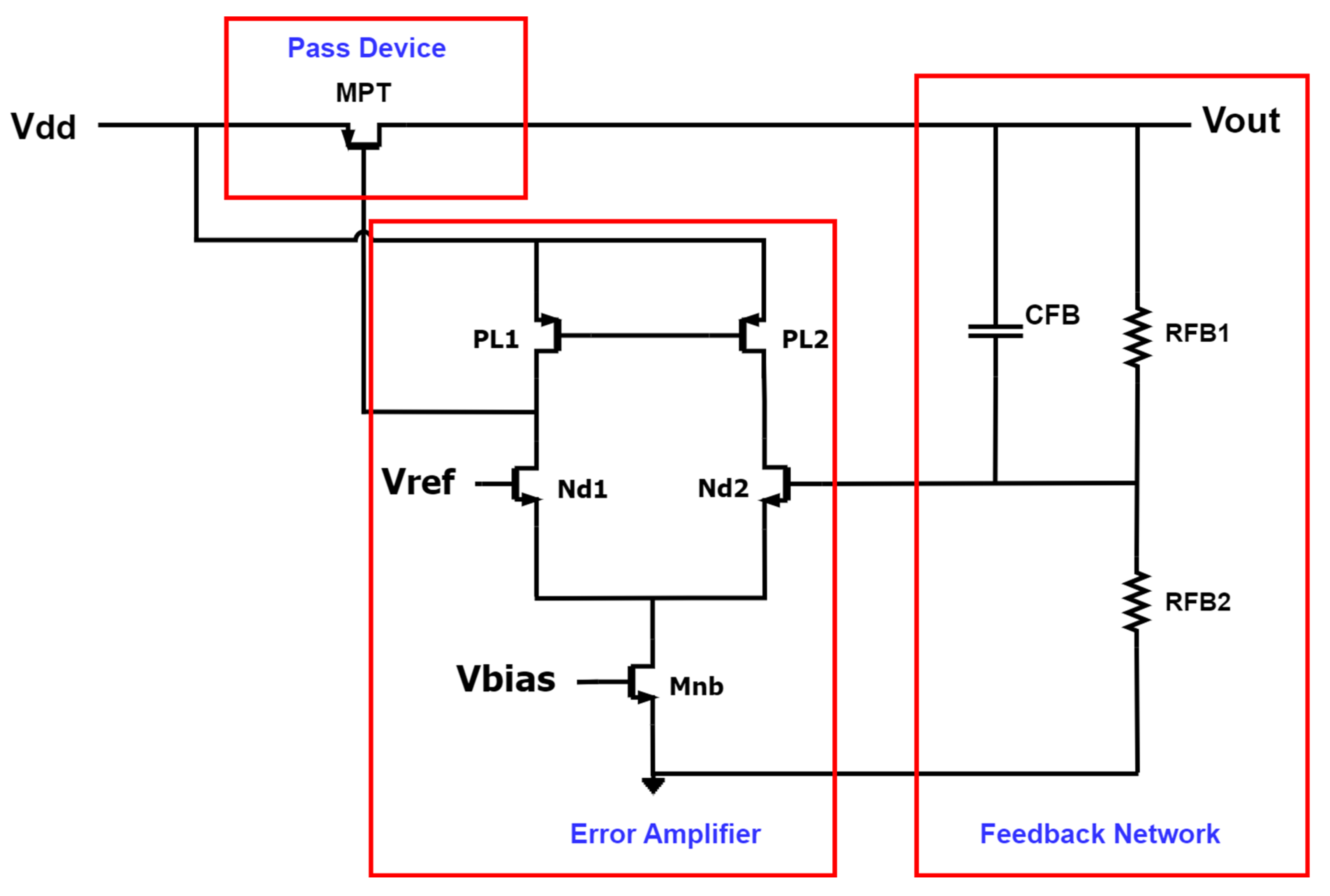
2. Design Concept and Implementation

The following equations present the loop analyses of the LDO design shown in Figure 1. The LDO output Vout shown in (3) is a function of two terms. The first term is due to the main feedback regulation loop as a function of Vref as shown in (1), and the second term is due to the feedforward path through MPT as a function of Vin as shown in (2).
V out / V r e f   =   g m , N d 1   ×   Z E A   ×   g m , M P T   ×   Z o u t / 1   +   β   ×   g m , N d 1   ×   Z E A   ×   g m , M P T   ×   Z o u t   =   A v L / [ 1   +   β   ×   A v L ] = [ g m , N d 1 × [ r o , E A / ( 1 + S × r o , E A     C o , E A ) ] × g m , M P T     Z o u t ] [ 1 + [ R F B 2 / ( R F B 1 + R F B 2 ) ] × g m , N d 1 × [ r o , E A / ( 1 + S × r o , E A × C o , E A ] × g m , M P T × Z o u t ]
V out / V d d   =   g m , M P T   ×   Z o u t / 1   +   β   ×   g m , N d 1   ×   Z E A   ×   g m , M P T   ×   Z o u t   =   A V P T / [ 1   +   β   ×   A v L ]   = [ g m , M P T Z o u t ] [ 1 + [ g m , N d 1     r o , E A     g m , M P T     Z o u t     R F B 2 ] / [ ( R F B 1 + R F B 2 )     ( 1 + ( s / ω E A ) ) ] ]
Vout ≈ Vref [AVL/(1 + β × AVL] + Vdd [AVPT/(1 + β × AVL]
AVL = gm,Nd1 × ZEA × gm,MPT × Zout
AVPT = gm,MPT × Zout
Zout = rout,MPT ⫽ RL ⫽ (RFB1 + RFB2)
ZEA = ro,EA  ⫽ (1/SCo,EA) = ro,EA/(1 + S × ro,EA × Co,EA)
β = RFB2/(RFB1 + RFB2)
where Vref is the reference voltage generated from the bandgap, AVL is the LDO’s loop gain, AVPT is the pass transistor stage’s gain, Zout is the overall output impedance of the LDO, ZEA is the error amplifier’s total output impedance, gm,MPT is the gm of the pass device, gm,Nd1 is the gm of the error amplifier’s input pair, and Co,EA is the total capacitance at the error amplifier output. The total capacitance includes drain capacitance at the input pair and load devices, as well as the effective gate capacitance of the pass device.
As shown in (1), at high frequencies (S = ∞) and due to the pole of the error amplifier, the TF goes to zero. Thus, the ripples through the error amplifier and bandgap do not appear at the output. While at a low frequency (S = 0), the PSR of the bandgap is amplified by the feedback ratio and affects the overall LDO output PSR. In (2), it is shown that at a low frequency (S = 0), the supply noise is not very effective because it is divided by the error amplifier gain multiplied by the feedback network factor. While at a high frequency (S = ∞), the supply noise is amplified by the pass device gain affecting the LDO PSR at high frequency. So, the low-frequency LDO PSR is dominated by the bandgap and error amplifier, while high-frequency LDO PSR is dominated by the supply noise through the pass device.

2.1. PSR Enhancement

From the loop analyses, the high-frequency PSR of the LDO is dominated by the pass device path. It can be increased by increasing rout of the pass device because of the larger high-frequency loop gain and PSR. Also, the PSR can be improved by increasing the supply noise coupling to the pass transistor gate. This is because the more the supply noise coupling to the pass device gate, the higher the noise cancellation due to source–gate cancellation. The supply noise appearing at the source has a positive common gate gain. While the noise coupled to the gate has a negative common source gain. The two gains cancel each other providing a higher high-frequency PSR at the output.
Based on that, a design that combines two techniques of PSR improvement for conventional LDOs is presented. The first compensation technique is based on our work in [22], it works on coupling the noise to the pass device gate through a feedforward load-dependent compensation circuit as described in Section 2.1.1. The second technique of compensation is based on our work in [23], which enhances the rout of the pass device (rout,MPT) as described in Section 2.1.2.

2.1.1. Feedforward Compensation PSR Improvement

Figure 2 shows the compensation circuit added to provide a path for the supply noise to the pass device gate to have high-frequency noise coupling. It presents a modified circuit for the design proposed in [23]. Mainly it pushes current through the circuit depending on the load current that flows through the pass device, providing the load-dependent feedforward compensation.
For low loads, rout,MPT of the pass device is large enough to provide a high PSR, while for a large load current, rout,MPT of the pass device is small with low loop gain and PSR. As a result, the PSR improvement circuit is mainly needed at high loads. The proposed circuit works depending on the load current passing through the pass device. The gates of the devices MP3 and the pass device MPT are connected to have the same Vsg. The width of MP3 is much smaller. Therefore, MP3 will act as a current mirror for the load current. At zero load current, MP3 is off, disabling the proposed circuit and leading to a low quiescent current. At large loads, the circuit works by providing a path from the supply to the gate of the pass device through the device MP1 and the capacitor CP. This improves the PSR at large load currents.
The proposed feedforward compensation adds the device MP1 in parallel to MpL1, which is the error amplifier load device. This decreases ro,EA, and hence the DC loop gain. Also, this affects the dc operating point of the main feedback loop. To avoid this issue, a capacitor CP is added to isolate the added feedforward circuit at DC as it behaves as an open circuit. While at a high frequency where the feedforward path is needed to improve the high-frequency PSR, CP becomes effective in connecting the path without affecting the DC operating point or the DC loop gain.
Also, the capacitor CC is added between MN1, the source of the device, which is a low impedance node, and the LDO output to generate a high frequency zero ωz,cc. This zero improves the PSR at the MHz frequency range and improves the stability across different load currents. This is because gm,MN1 also depend on the mirrored current by MP3. So, the zero location now depends on the LDO load current. The higher load current will lead to higher gm,MN1, and hence better high-frequency PSR at ωz,cc, where:
ωz,cc ⍺ gm,N1
The modification made to our work in [22] is removing three devices in the feedforward circuit that were used for biasing MP1, making use of the bandgap circuit that already generates Vref and Vnbias. The bias Vpbias for MP1 can be externally generated without these three devices. This decreases the circuit area and removes the power consumption through the removed branch at a large load current of 15 µA instead of 18 µA at 200 mA.
The LDO loop gain analyses with the feedforward loop are derived based on the LDO shown in Figure 2. As the load current increases, the feedforward loop gain Avff increases due to higher gm,MP1 as shown in (11). This helps in amplifying the supply noise on the gate of the pass device and improving the noise cancellation with a higher PSR at the high-frequency path. The LDO output shown in (3) becomes a function of the feedforward path gain through CP as Equation (10) shows.
VOut ≈ Vref ((AVL)/(1 + β × AVL)) + Vdd ((AVPT (1 − AVff/ZCp))/(1 + β × AVL))
AVff = gm,P1 × (rout,P1 ⫽ (gm,N1 × rout,N1 × rout,N2))
ZCP = 1/(S × CP)
The output function of the LDO shown in (10) guarantees that the proposed loop improves PSR and the overall gain due to AVff term at high frequencies where ZCP becomes effective. AVff is the feedforward loop gain, and ZCP is the impedance of the capacitor CP.

2.1.2. Loop Gain Adjustment for PSR Improvement

The LDO’s loop gain increases with rout,MPT as shown in (4)–(6). Increasing the length of the pass device MPT increases rout,MPT and the high-frequency PSR. But this affects the DC loop operating point since it increases the voltage drop on the pass device which limits the DC load current that the LDO can support due to lower W/L of the pass device. A technique that increases r o u t , M P T at high frequency and hence the high-frequency PSR is shown in Figure 3.
Adding another series device (HPT) with the main pass device MPT increases the overall pass device length, which increases rout,MPT and improves the high-frequency PSR. The gate of the device HPT is connected to the error amplifier output through the capacitor CHF, which acts as a short circuit at high frequencies to provide a larger length to the pass device due to two cascode devices, MPT and HPT. This improves the high-frequency loop gain and PSR. CHF is an open circuit at DC isolating the added device HPT from the main loop by pulling the gate of HPT to the ground through an off-transistor MRHF that acts as a large resistor. This makes HPT act as a short circuit at DC. Thus, the main device MPT will only work by providing sufficient dropout for the large load current. The analyses of the proposed circuit show that Zout keeps the same at DC but increases at high frequency due to the cascode to be:
Zout.HF = gm,MPT × rout,MPT × rout,HPT ⫽ RL ⫽ (RFB1 + RFB2)
The modification completed on our work in [23] is to replace a very large resistor RHF with a small off-transistor MRHF to act as a large resistor to pull down HPT’s gate to ground at DC but with much smaller area consumption.

2.2. Inrush Current Improvement

A common issue for capped LDO is the inrush current that can cause electromigration and IR-drop “EMIR” issues. At large load capacitor values, Vout is charged by “dVout” within time “dTch” according to (14) where:
CLoad × dVout = ILoad × dTch
For large CLoad, the slow charging time of Vout makes Vfb, which is the positive input of the error amplifier rise slower than Vref, which is the negative input making the amplifier output “pass transistor gate” low. This increases Vsg on the pass transistor for an interval until Vfb comes up closer to Vref and the loop works normally. Having a large W/L pass device due to large load currents with such very large Vsg during start-up provides a large inrush current.
An effective solution is to split the main pass device MPT into two parallel devices as shown in Figure 4, which shows the final proposed LDO design. The first is an always enabled small one (MPTS) “small W/L”, and the second is a larger one (MPTL) that is enabled after the RC filter (RF and CF) delay is larger than the inrush current interval. This limits the inrush current due to enabling the smaller pass device at start-up then enabling MPTL after the RC delay makes the loop operate normally with the whole pass device size to support the whole load current. The added RC pole does not affect the stability as it is at a much higher frequency.

2.3. Techniques for Stability Compensation

The newly proposed LDO is stable for a wide range of load currents up to 200 mA and a capacitor range from 1 nF to 12 µF. The device HPT improves the stability as it increases Zout at high frequencies as shown in (13) by decreasing the dominant pole at the LDO output. The newly proposed LDO shows higher phase margin values compared to the work completed in [22] which includes a similar idea of the feedforward loop, with smaller compensation devices CP and CC, which decreases the area.
At different load currents, the poles ωpout and ωpEA will change their locations as both are functions of load currents. The zero ωz,cc will change its location depending on the output load current according to (9) and follows the non-dominant pole change. This provides compensation to keep the system stable for a load current range from 0 to 200 mA.

3. Simulation Results

The layout of the newly proposed LDO is shown in Figure 5. The silicon area consumption is 180 µm × 180 µm. The RCC post-layout view of the LDO is verified with different load capacitors and different load currents with a bandgap that generates the reference and the bias voltages Vref, Vnbias, and Vpbias. Electric series inductance “ESL” and electric series resistance “ESR” are added at different load capacitors based on the capacitor value. At 3 V supply, 4 µF load capacitor, and 25 mA load current, transient results are presented in Figure 6. The supply ramps to 3 V while Vref ramps to 1.2 V. The LDO output ramps and settles as expected at 1.8 V.

3.1. PSR Simulations

The high-frequency improvement in PSR is presented in Figure 7 after each stage of compensation. PSR at the DC of the LDO is not affected by the two proposed high-frequency PSR compensation techniques—the same for the DC operating point and the loop DC gain.
Figure 7 shows the PSR improvement at 100 kHz, 1 MHz, 10 MHz, and 30 MHz of each stage of compensation. The numbers are shown in Table 1.

3.2. Stability Measurements

Figure 8 presents the phase margin using different load capacitor values from 1 nF to 12 µF with their corresponding ESR and ESL models with load current ranging from 0 to 200 mA, all across process, voltage, and temperature conveniently called “PVT”. Where VDD is in the range of 2 V to 3 V, fast NMOS and PMOS and slow NMOS and PMOS for process corners, a low temperature of −40 °C and 125 °C for maximum temperature, it shows a worst phase margin of 51 degrees.

3.3. Inrush Current Improvement

Ram** the LDO supply from 0 to 3 V in 30 µs shows inrush current improvement by more than 2× from 120 mA to 58 mA using the proposed design as shown in Figure 9.
Table 2 compares between this work and previous works, using a figure of merit (FOM) for an overall comparison as shown in (15). The newly proposed LDO has the best FOM across different high frequencies.
FOM = 10 × log((|PSR| × ILoad@psr))/(Iq × CL@psr) × Area))
PSR is in dB, iLoad is in mA, Iq in µA, CL in µF, and the area is in mm2.

4. Conclusions

In this work, we presented an innovative LDO design that includes two compensation techniques to be utilized in LDOs that improve its high-frequency PSR and loop stability without adding a complex loop that degrades the power and the area consumption. The two techniques improve the design PSR by providing a load-dependent feedforward noise path to the pass device gate and adjusting the loop gain at different frequencies. In addition, it guarantees loop stability over a wide load current range from 0 to 200 mA and a wide load capacitor range from 1 nF to 12 µF. The design provides a big improvement in the LDO output PSR by up to −50 dB at 10 MHz and −53 dB at 30 MHz. Also, it shows a technique that improves the LDO inrush current during startup by more than 2X with much smaller power and area compared to previous works in the literature.

Author Contributions

Conceptualization, H.H.H.; Methodology, H.H.H.; Validation, H.H.H.; Formal analysis, H.H.H.; Investigation, H.H.H.; Resources, H.H.H.; Writing—original draft, H.H.H. and M.A.H.; Writing—review & editing, H.H.H. and M.A.H.; Visualization, M.A.H.; Supervision, H.A.O. and S.A.I. All authors have read and agreed to the published version of the manuscript.

Funding

This research received no external funding.

Informed Consent Statement

Not Applicable.

Data Availability Statement

Conflicts of Interest

The authors declare no conflict of interest.

References

  1. Gupta, V.; Rincon-Mora, G.A.; Raha, P. Analysis and design of monolithic, high PSR, linear regulators for SoC applications. In Proceedings of the IEEE International SOC Conference, 2004. Proceedings, Santa Clara, CA, USA, 12–15 September 2004. [Google Scholar]
  2. Gupta, V.; Rincon-Mora, G.A. A Low Dropout, CMOS Regulator with High PSR over Wideband Frequencies. In Proceedings of the 2005 IEEE International Symposium on Circuits and Systems, Kobe, Japan, 23–26 May 2005. [Google Scholar]
  3. El-Nozahi, M.; Amer, A.; Torres, J.; Entesari, K.; Sanchez-Sinencio, E. High PSR Low Drop-Out Regulator With Feed-Forward Ripple Cancellation Technique. IEEE J. Solid-State Circuits 2010, 45, 565–577. [Google Scholar] [CrossRef]
  4. Yuk, Y.; Jung, S.; Kim, C.; Gwon, H.; Choi, S.; Cho, G. PSR Enhancement through Super Gain Boosting and Differential Feed-Forward Noise Cancellation in a 65-nm CMOS LDO Regulator. IEEE Trans. Very Large Scale Integr. (VLSI) Syst. 2014, 22, 2181–2191. [Google Scholar] [CrossRef]
  5. Jiang, J.; Shu, W.; Chang, J.S. A 65-nm CMOS Low Dropout Regulator Featuring >60-dB PSRR Over 10-MHz Frequency Range and 100-mA Load Current Range. IEEE J. Solid-State Circuits 2018, 53, 2331–2342. [Google Scholar] [CrossRef]
  6. Chen, L.; Cheng, Q.; Guo, J.; Chen, M. High-PSR CMOS LDO with embedded ripple feedforward and energy-efficient bandwidth extension. In Proceedings of the 2015 28th IEEE International System-on-Chip Conference (SOCC), Bei**g, China, 8–11 September 2015; pp. 384–389. [Google Scholar]
  7. Joshi, K.; Manandhar, S.; Bakkaloglu, B. A 5.6 μ a Wide Bandwidth, High Power Supply Rejection Linear Low-Dropout Regulator with 68 dB of PSR up to 2 MHz. IEEE J. Solid-State Circuits 2020, 55, 2151–2160. [Google Scholar] [CrossRef]
  8. Hipolito, C.R.; Silverio, A.; Nuestro, R. High PSR LDO with Adaptive-EFFRC for Wearable Biomedical Application. In Proceedings of the 2021 IEEE International Symposium on Circuits and Systems (ISCAS), Daegu, Republic of Korea, 22–28 May 2021; pp. 1–5. [Google Scholar] [CrossRef]
  9. Li, R.; Zeng, Y.; Lin, Y.; Yang, J.; Tan, H.-Z. High-PSR and fast-transient LDO regulator with nested adaptive FVF structure. In Proceedings of the 2020 IEEE International Conference on Integrated Circuits, Technologies and Applications (ICTA), Nan**g, China, 23–25 November 2020; pp. 51–52. [Google Scholar] [CrossRef]
  10. Kim, D.-K.; Shin, S.-U.; Kim, H.-S. A BGR-Recursive Low-Dropout Regulator Achieving High PSR in the Low- to Mid-Frequency Range. IEEE Trans. Power Electron. 2020, 35, 13441–13454. [Google Scholar] [CrossRef]
  11. Chen, J.; Luo, P.; Wang, H.; He, Z.; Song, H. A high PSR LDO with adaptive loop switching control and feedforward ripple cancellation techniques. AEU Int. J. Electron. Commun. 2022, 155, 154355. [Google Scholar] [CrossRef]
  12. Niu, Z.; Lai, X.; Wang, B. A Wide Input Voltage Range, High PSR Low-Dropout Regulator with a Closed-Loop Charge Pump for Sensor Front-End Circuits. Authorea 2023. [Google Scholar] [CrossRef]
  13. Lavalle-Aviles, F.; Torres, J.; Sánchez-Sinencio, E. A High-Power Supply Rejection and Fast Settling Time Capacitor-Less LDO. IEEE Trans. Power Electron. 2019, 34, 474–484. [Google Scholar] [CrossRef]
  14. Pérez-Bailón, J.; Calvo, B.; Medrano, N. A Fully Integrated 180 nm CMOS 1.2 V Low-Dropout Regulator for Low-Power Portable Applications. Electronics 2021, 10, 2108. [Google Scholar] [CrossRef]
  15. Kakhki, A.P.; Maymandi-Nejad, M. A low dropout regulator with enhanced power supply rejection and stability. In Proceedings of the 2017 Iranian Conference on Electrical Engineering (ICEE), Tehran, Iran, 2–4 May 2017; pp. 387–391. [Google Scholar] [CrossRef]
  16. Choe, Y.-J.; Nam, H.; Park, J.-D. A Low-Dropout Regulator with PSRR Enhancement through Feed-Forward Ripple Cancellation Technique in 65 nm CMOS Process. Electronics 2020, 9, 146. [Google Scholar] [CrossRef] [Green Version]
  17. Zarate-Roldan, J.; Wang, M.; Torres, J.; Sánchez-Sinencio, E. A Capacitor-Less LDO With High-Frequency PSR Suitable for a Wide Range of On-Chip Capacitive Loads. IEEE Trans. Very Large-Scale Integr. (VLSI) Syst. 2016, 24, 2970–2982. [Google Scholar] [CrossRef]
  18. Lim, Y.; Lee, J.; Lee, Y.; Song, S.S.; Kim, H.T.; Lee, O.; Choi, J. An External Capacitor-Less Ultralow-Dropout Regulator Using a Loop-Gain Stabilizing Technique for High Power-Supply Rejection Over a Wide Range of Load Current. IEEE Trans. Very Large-Scale Integr. (VLSI) Syst. 2017, 25, 3006–3018. [Google Scholar] [CrossRef]
  19. Lim, Y.; Lee, J.; Park, S.; Jo, Y.; Choi, J. An External Capacitorless Low-Dropout Regulator with High PSR at All Frequencies From 10 kHz to 1 GHz Using an Adaptive Supply-Ripple Cancellation Technique. IEEE J. Solid-State Circuits 2018, 53, 2675–2685. [Google Scholar] [CrossRef]
  20. Li, G.; Qian, H.; Guo, J.; Mo, B.; Lu, Y.; Chen, D. Dual Active-Feedback Frequency Compensation for Output-Capacitorless LDO with Transient and Stability Enhancement in 65-nm CMOS. IEEE Trans. Power Electron. 2020, 35, 415–429. [Google Scholar] [CrossRef]
  21. Li, Y.; Wang, L.; Wang, Y.; Wang, S.; Cui, M.; Guo, M. A Low-Power, Fast-Transient FVF-Based Output-Capacitorless LDO with Push–Pull Buffer and Adaptive Resistance Unit. Electronics 2023, 12, 1285. [Google Scholar] [CrossRef]
  22. Hammam, H.H.; Omran, H.A.; Ibrahim, S.A. A Low Power High PSR Wide Load LDO With Load-Dependent Feedforward Cancellation Technique. In Proceedings of the 2021 IEEE International Midwest Symposium on Circuits and Systems (MWSCAS), Lansing, MI, USA, 9–11 August 2021. [Google Scholar]
  23. Hammam, H.H.; Omran, H.A.; Ibrahim, S.A. Ultra-Low-Power Low Drop-Out (LDO) Voltage Regulator with Improved Power Supply Rejection. In Proceedings of the 2021 38th National Radio Science Conference (NRSC), Mansoura, Egypt, 27–29 July 2021. [Google Scholar]
Figure 1. Transistor level diagram of conventional LDO.
Eng 04 00120 g001
Figure 2. PSR improvement using feedforward loop and compensation capacitors.
Eng 04 00120 g002
Figure 3. LDO design with 2 stages of PSR compensations.
Eng 04 00120 g003
Figure 4. The proposed LDO design with PSR and inrush current improvement.
Eng 04 00120 g004
Figure 5. The layout of the LDO.
Eng 04 00120 g005
Figure 6. The proposed LDO transient simulations.
Eng 04 00120 g006
Figure 7. PSR of conventional LDO, first stage of the feedforward compensation, and the second stage of loop gain compensation.
Eng 04 00120 g007
Figure 8. Phase margin across PVT, iLoad, and CLoad.
Eng 04 00120 g008
Figure 9. Inrush current for conventional and proposed LDOs.
Eng 04 00120 g009
Table 1. Comparison between PSR at different frequencies.
FrequencyConventional LDOAfter Adding 1st
Compensation
After Adding 2nd
Compensation
100 kHz−65 dB−76 dB−78 dB
1 MHz−40 dB−78 dB−82 dB
10 MHz−32 dB−72 dB−83 dB
30 MHz−30 dB−70 dB−83 dB
Table 2. Comparison between the proposed LDO and the previously published LDOs.
[3][4][6][5][7][22][23]This Work
Year20102014201520182020202120212023
Technology (nm)1306518065180656565
Active Area (mm2)0.0490.0360.210.0480.120.0360.080.0324
Input Voltage (V)>1.151.15–1.31.31.25>22.7–3.3>2
Output Voltage (V)111.214.51.81.81.8
Maximum iLoad (mA)252525100250200100200
Output Capacitor (µF)44–4.74.74.71–120.001–121–120.001–12
Quiescent current (µA)40150–35010405.6–35.610–18510–15
PSRR (Power Supply Rejection Ratio) (dB)@4 µF,@4 µF,@4.7 µF,@4.7 µF,@2.2 µF,@4 µF,@4 µF,@4 µF,
@25 mA@25 mA@25 mA@100 mA@20 mA@25 mA@25 mA@25 mA
−60−65−71−89−77−80−77−78
@100 k@100 k@100 k@100 k@100 k@100 k@100 k@100 k
−67−61−69−70−72−83−85@−82
@1 M@1 M@1 M@1 M@1 M@1 M1 M@1 M
−56−47−63−62−62−82−80@−83
@10 M@10 M@10 M@10 M@10 M@10 M10 M@10 M
FOM@100 KHz22.818.7622.5529.9430.1831.4330.831.77
FOM@1 Mz23.318.4522.42528.929.8931.6931.2331.99
FOM@10 MHz22.5217.3622.0328.3729.2431.5330.9732
Disclaimer/Publisher’s Note: The statements, opinions and data contained in all publications are solely those of the individual author(s) and contributor(s) and not of MDPI and/or the editor(s). MDPI and/or the editor(s) disclaim responsibility for any injury to people or property resulting from any ideas, methods, instructions or products referred to in the content.

