
Graphene Coated Nanoprobes: A Review

Abstract
:1. Introduction
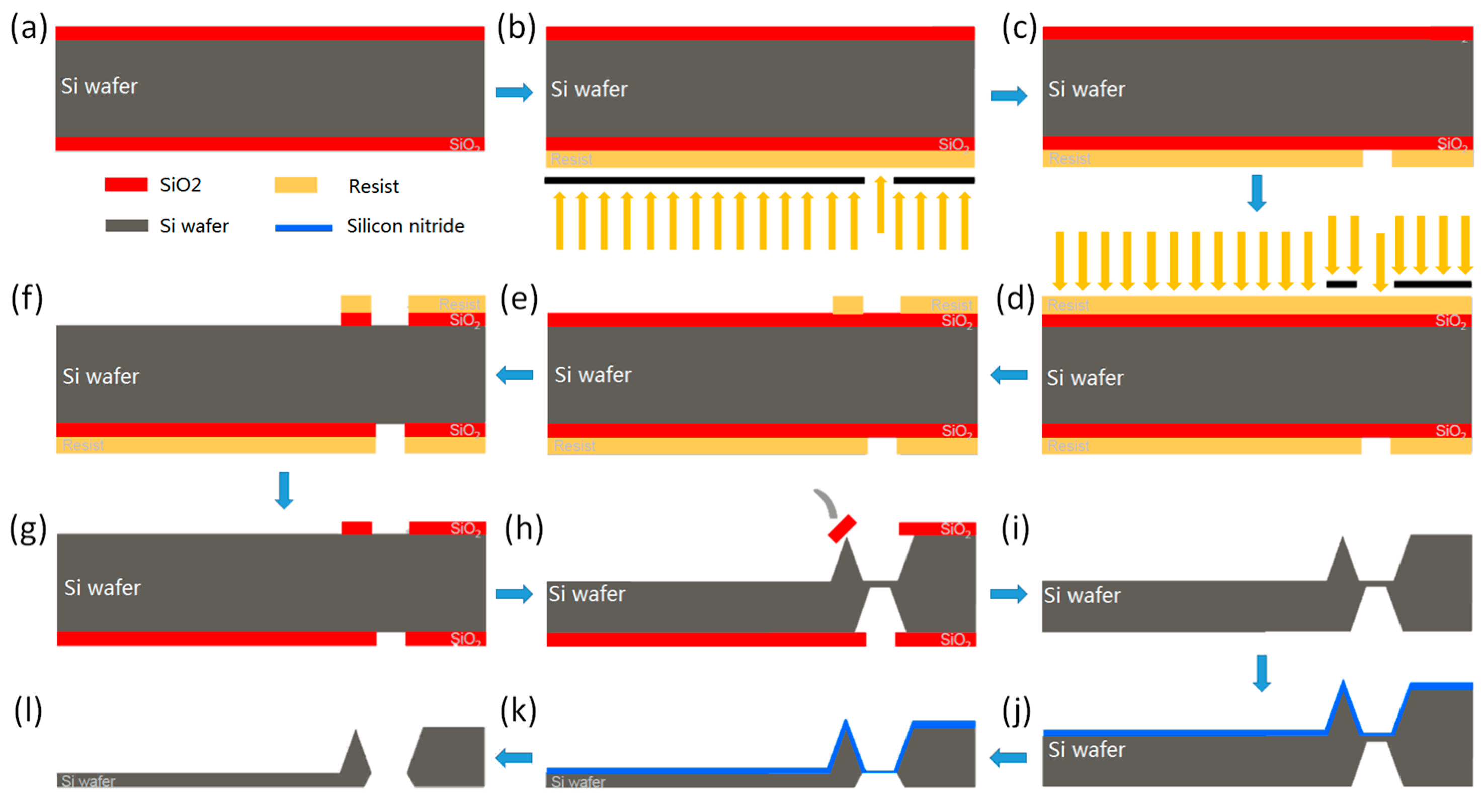
2. Graphene-Coated AFM Probes Production
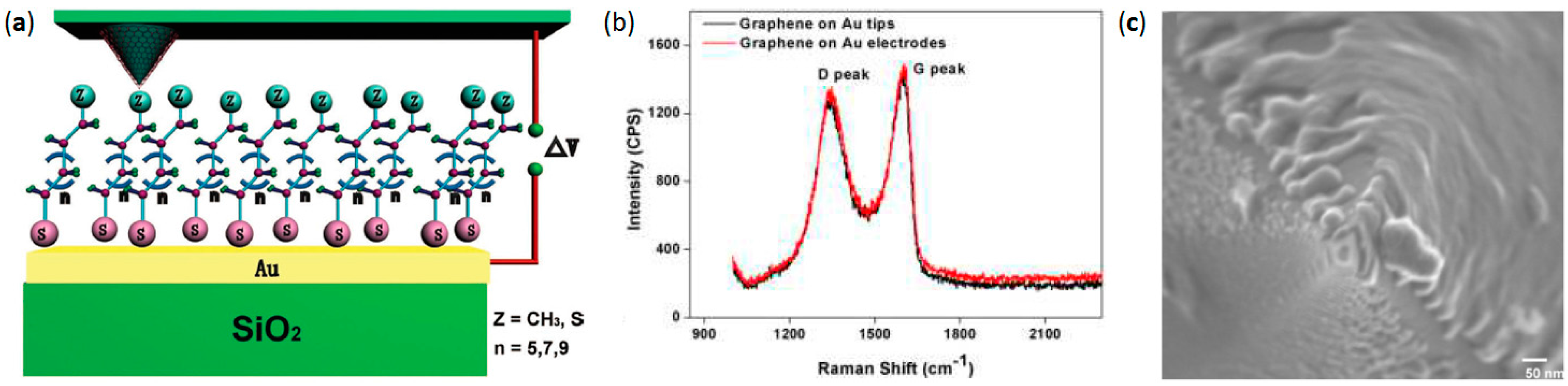
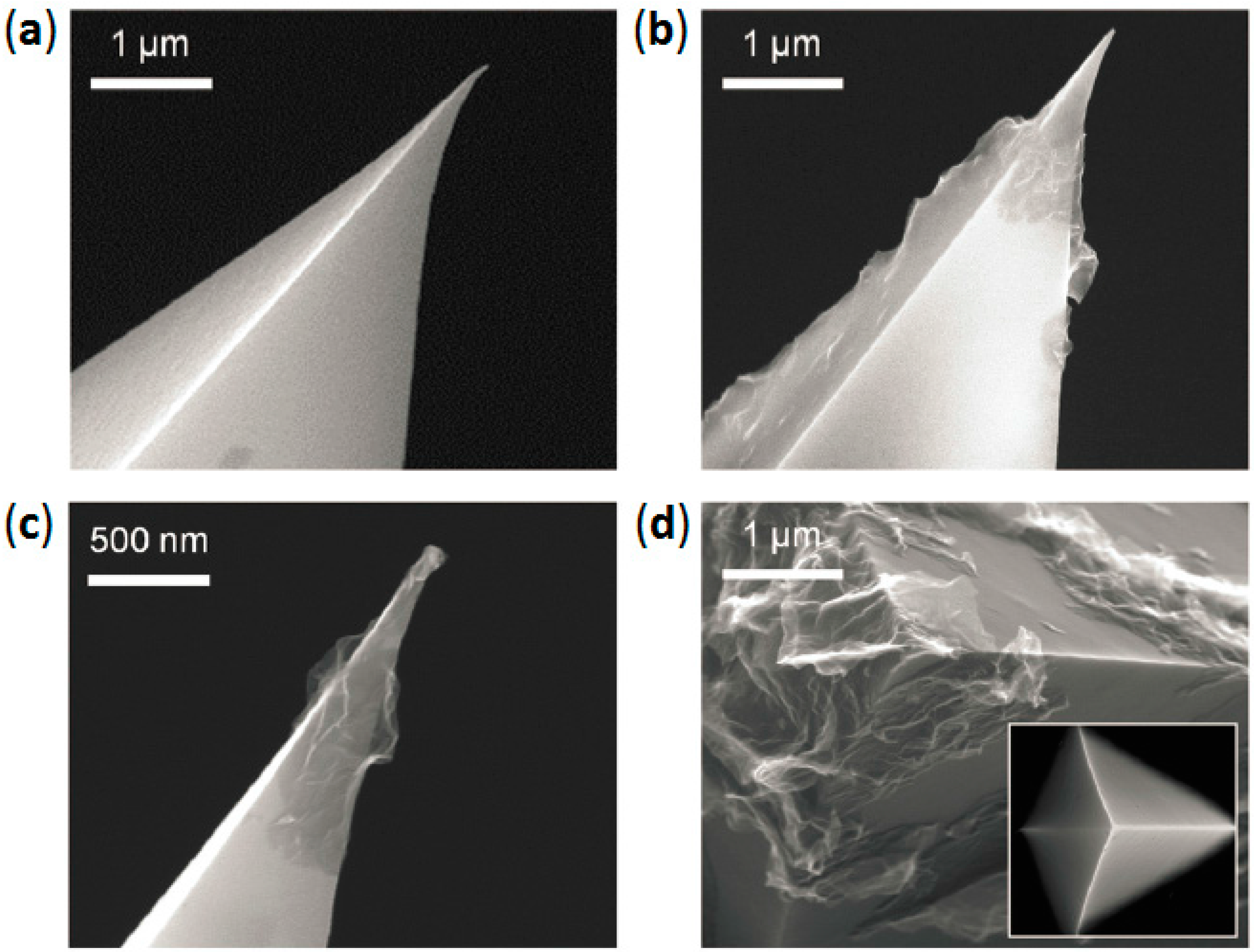
2.1. Direct Chemical Vapor Deposition of Graphene on AFM Nanoprobes
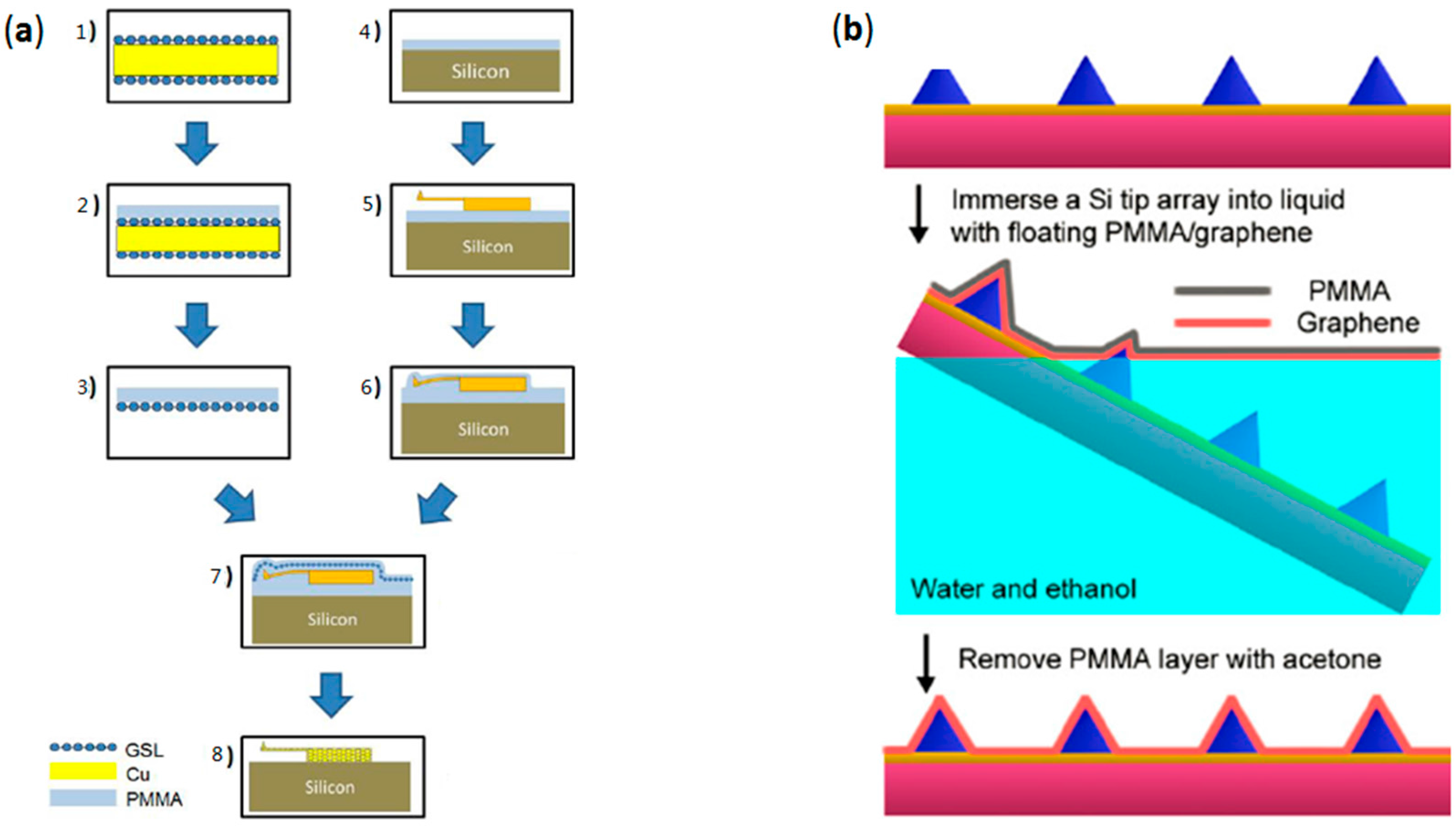
2.2. Transfer of CVD-Grown Graphene onto AFM Probes
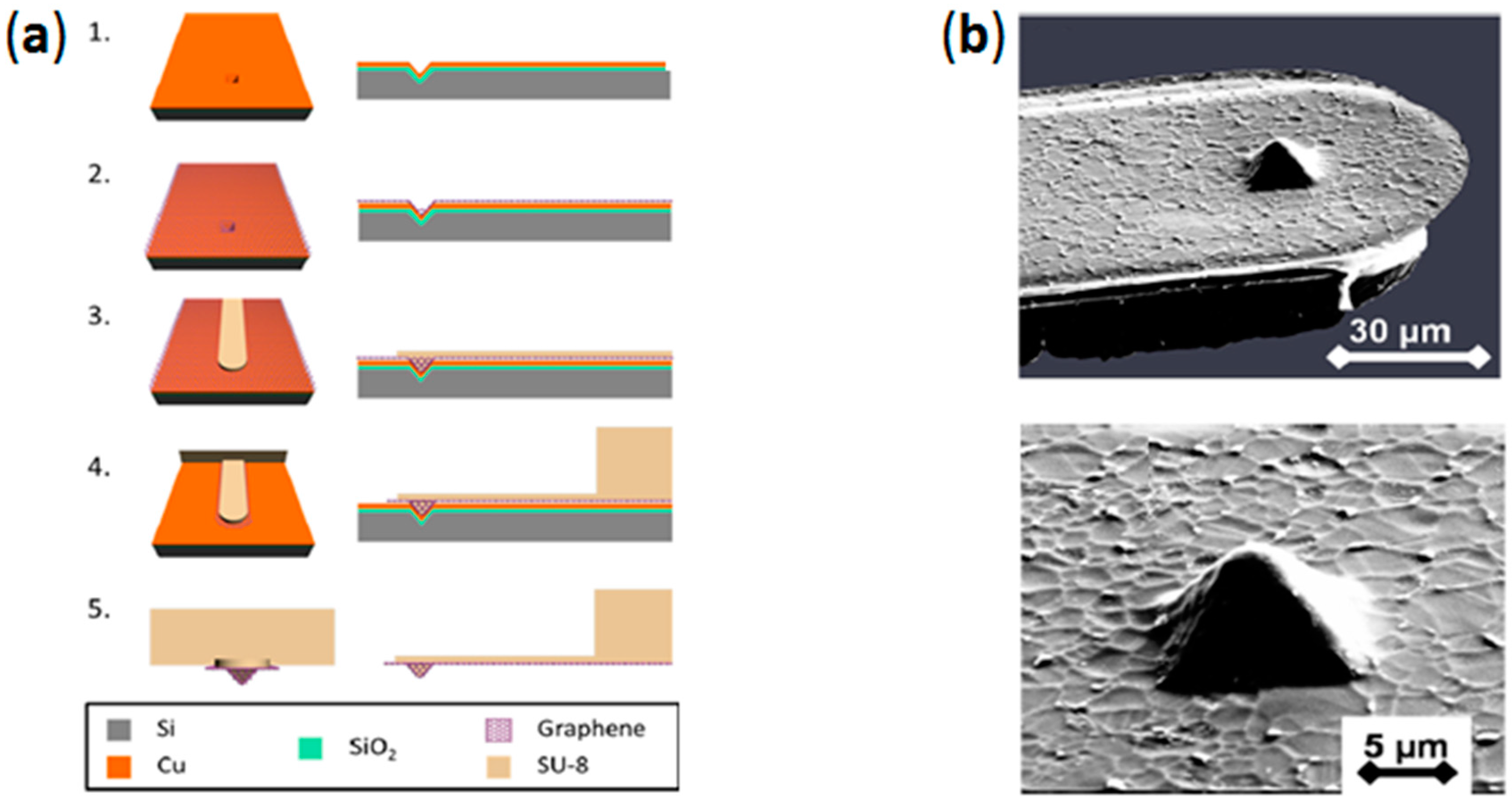
2.3. Mold-Assisted Transfer of CVD-Grown Graphene onto AFM Probes
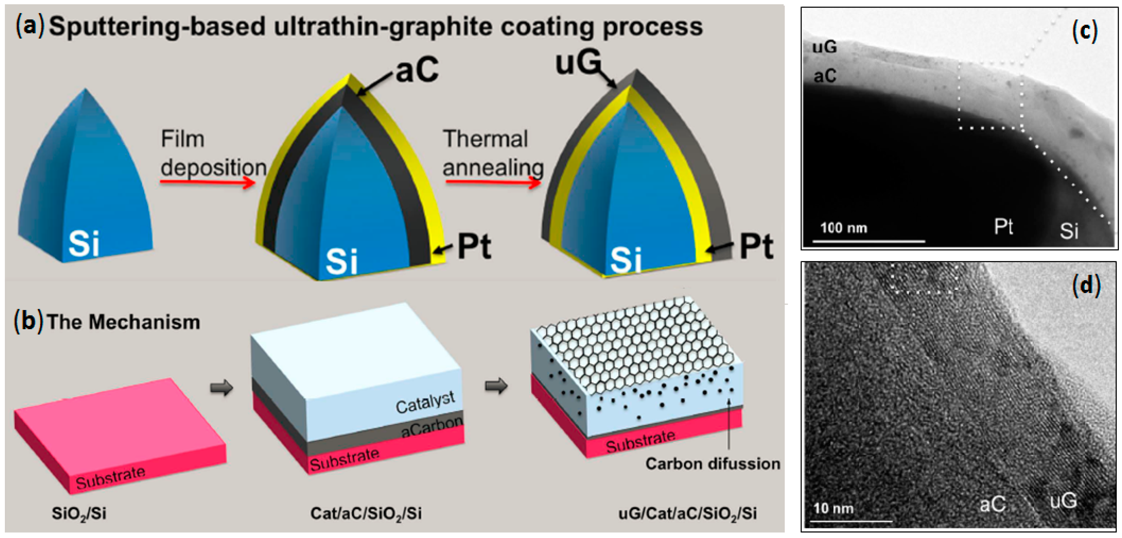
2.4. Direct Graphite-Like Thin Film Deposition on AFM Nanoprobes
2.5. Liquid Phase Graphene Flakes Coated AFM Probes
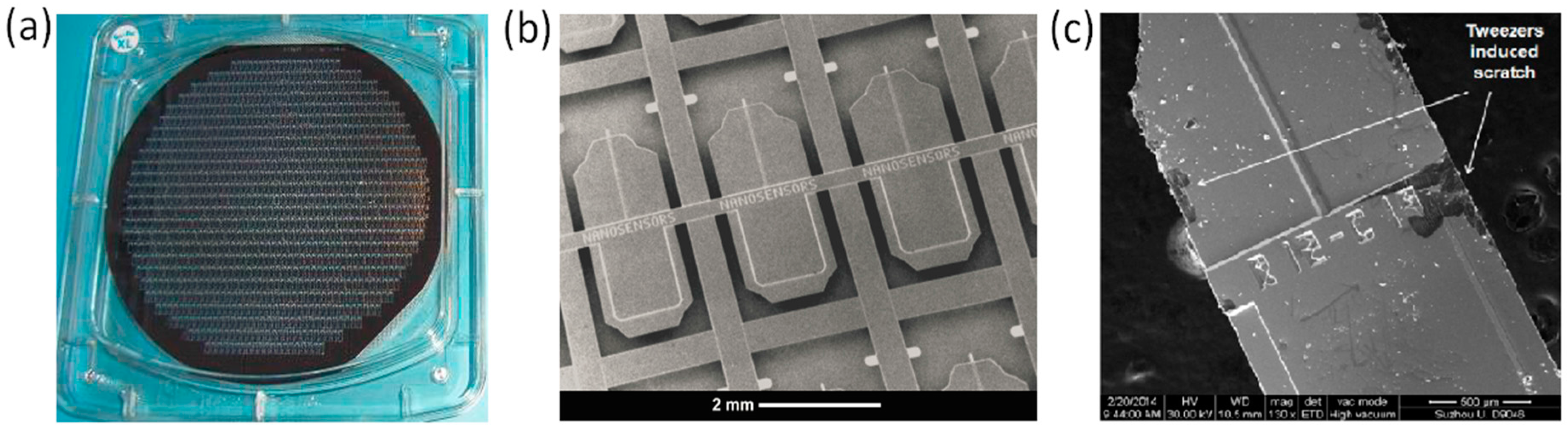
3. Perspectives on the Fabrication of Graphene Coated AFM Probes
4. Functionalities of Graphene Coated AFM Probes
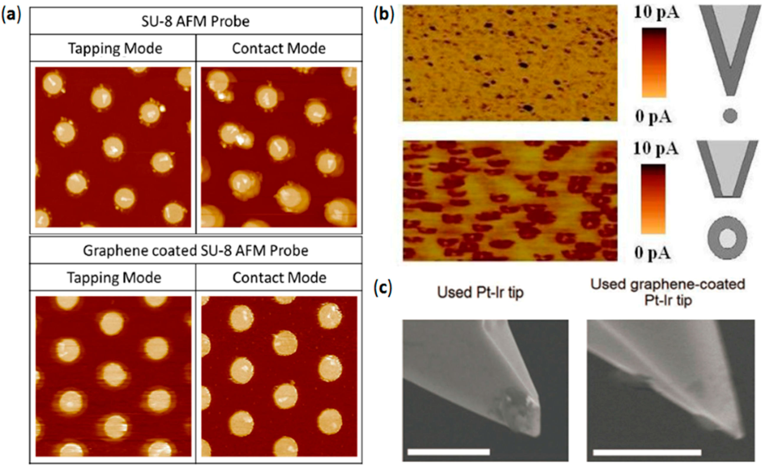
4.1. High Wear Resistance in Lateral Scans
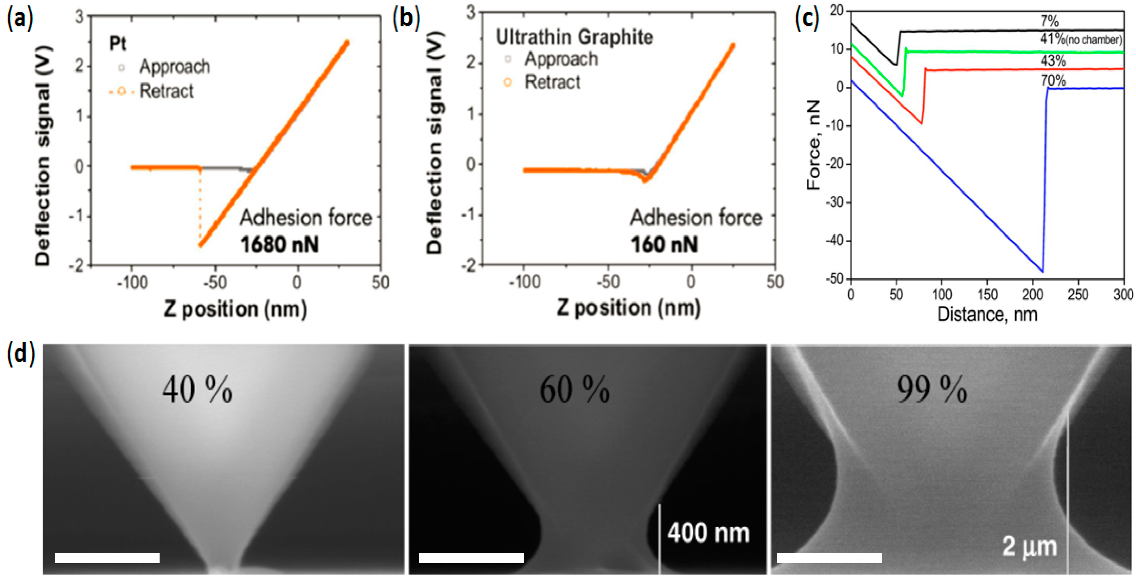
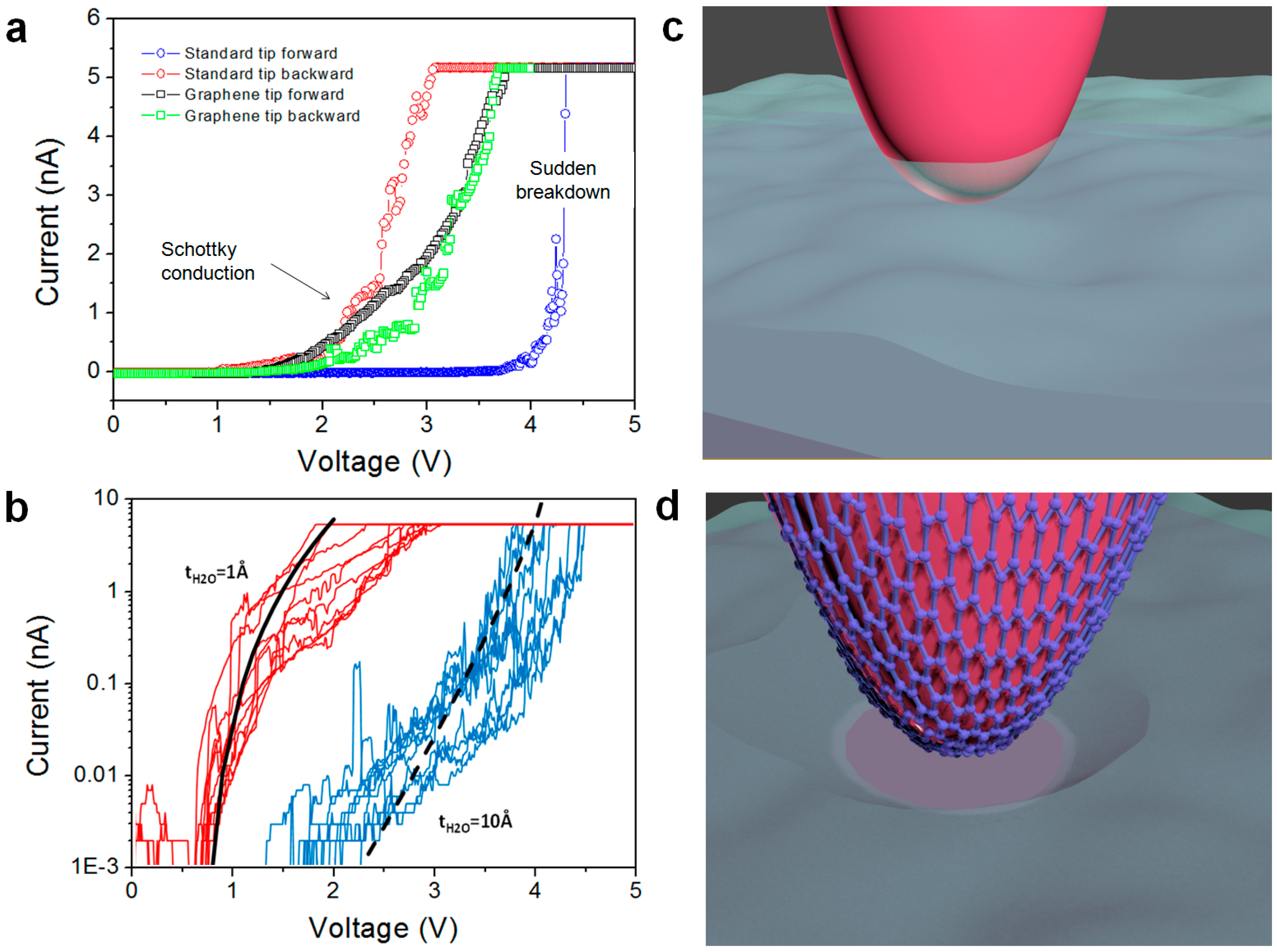
4.2. Avoiding Water Perturbations at the Tip–Sample Junction
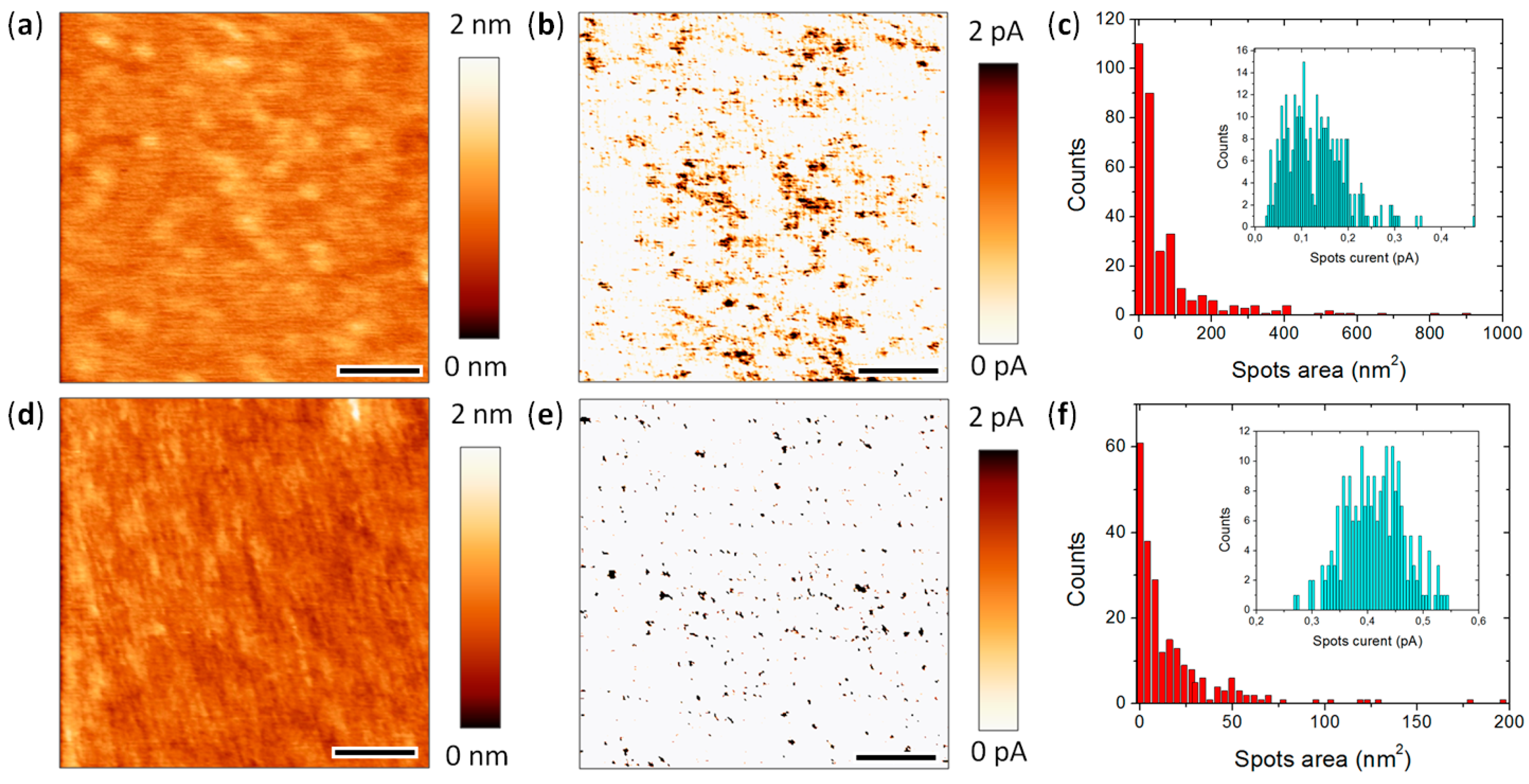
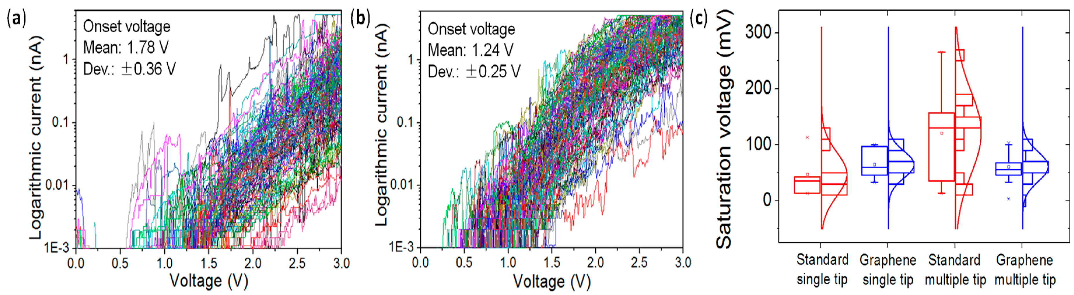
4.3. Lower Data Variability
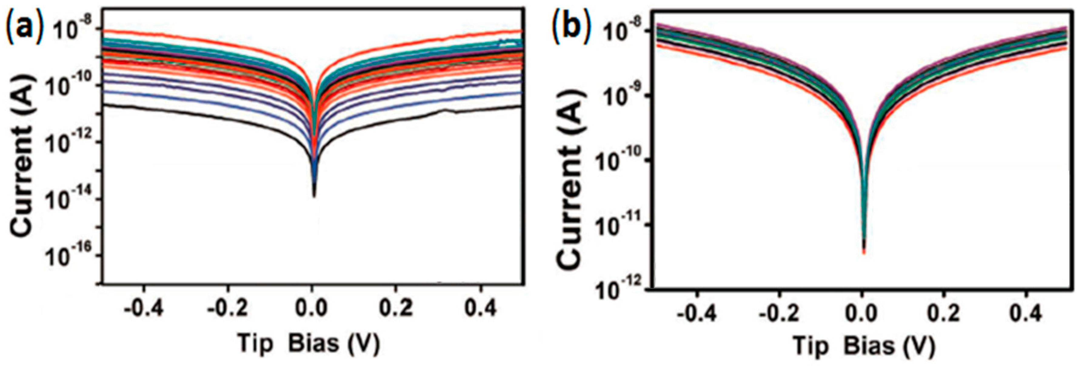
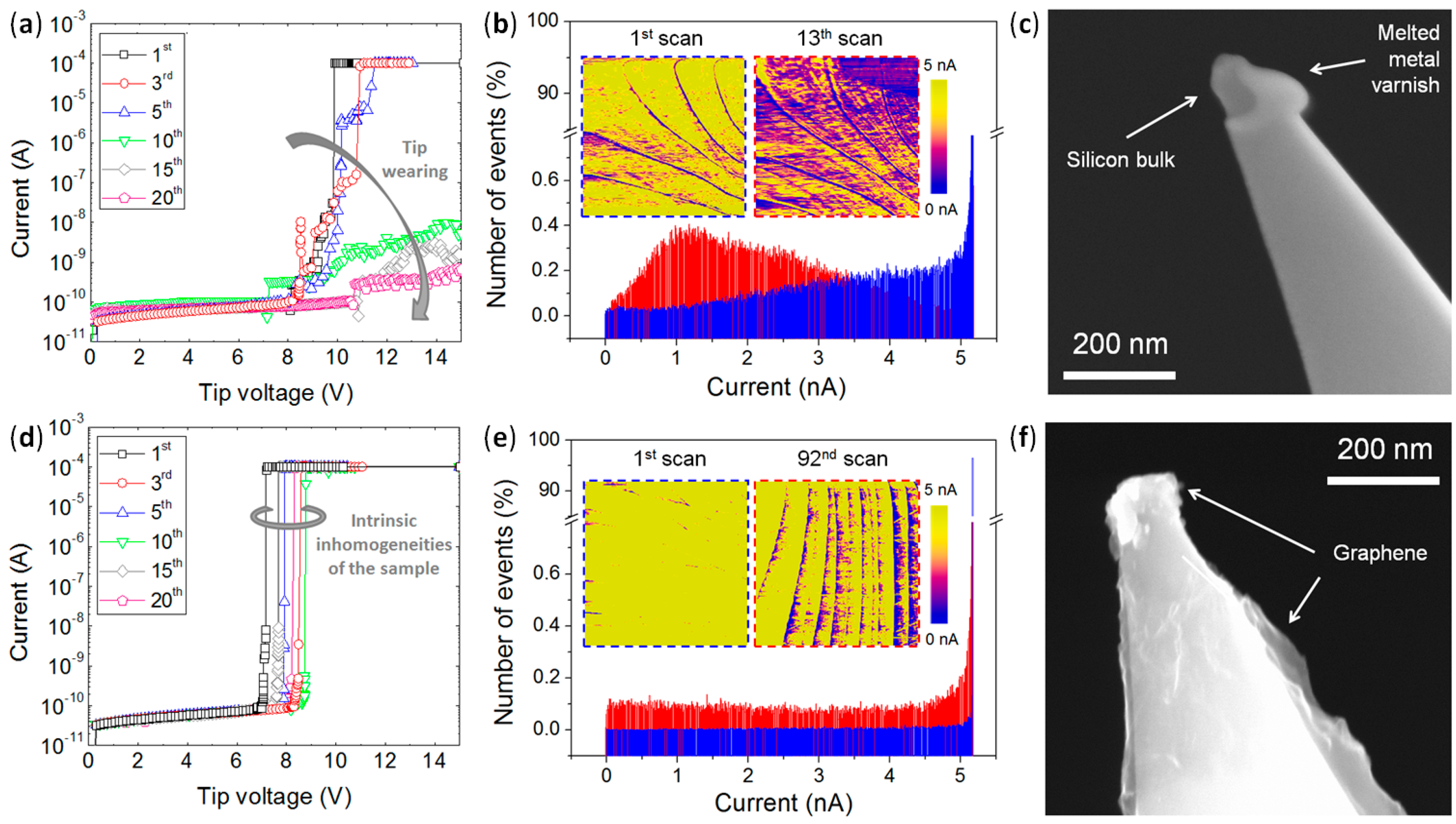
4.4. High Stability vs. High Currents and Mechanical Strains: Enhanced Lifetime
5. Conclusions
Acknowledgments
Conflicts of Interest
References
- Ji, Y.; Pan, C.; Zhang, M.; Long, S.; Lian, X.; Miao, F.; Hui, F.; Shi, Y.; Larcher, L.; Wu, E.; et al. Boron nitride as two dimensional dielectric: reliability and dielectric breakdown. Appl. Phys. Lett. 2016, 108, 012905. [Google Scholar] [CrossRef]
- Song, X.; Hui, F.; Gilmore, K.; Wang, B.; **g, G.; Fan, Z.; Grustan-Gutierrez, E.; Shi, Y.; Lombardi, L.; Hodge, S.A.; et al. Enhanced piezoelectric effect at the edges of stepped molybdenum disulfide. Nanoscale 2017, 9, 6237–6245. [Google Scholar] [CrossRef] [PubMed]
- Paxton, W.F.; Spruell, J.M.; Stoddart, J.F. Heterogeneous catalysis of a copper-coated atomic force microscopy tip for direct-write click chemistry. J. Am. Chem. Soc. 2009, 131, 6692–6694. [Google Scholar] [CrossRef] [PubMed]
- Park, K.D.; Raschke, M.B.; Jang, M.J.; Kim, J.H.; O, B.H.; Park, S.G.; Lee, E.H.; Lee, S.G. Near-field imaging of cell membranes in liquid enabled by active scanning probe mechanical resonance control. J. Phys. Chem. C. 2016, 120, 21138–21144. [Google Scholar] [CrossRef]
- Pan, N.; Rao, W.; Standke, S.J.; Yang, Z. Using dicationic ion-pairing compounds to enhance the single cell mass spectrometry analysis using the single-probe: A microscale sampling and ionization device. Anal. Chem. 2016, 88, 6812–6819. [Google Scholar] [CrossRef] [PubMed]
- Bining, G.; Quate, C.F.; Gerber, C. Atomic Force Microscope. Phys. Rev. Lett. 1986, 56, 930–933. [Google Scholar] [CrossRef] [PubMed]
- Kawahara, K.; Shirasawa, T.; Lin, C.L.; Nagao, R.; Tsukahara, N.; Takahashi, T.; Arafune, R.; Kawai, M.; Takagi, N. Atomic structure of “multilayer silicene” grown on Ag(111): Dynamical low energy electron diffraction analysis. Surf. Sci. 2016, 651, 70–75. [Google Scholar] [CrossRef]
- Hafner, J.H.; Cheung, C.L.; Woolley, A.T.; Lieber, C.M. Structural and functional imaging with carbon nanotube AFM probes. Prog. Biophys. Mol. Biol. 2001, 77, 73–110. [Google Scholar] [CrossRef] [Green Version]
- Yapici, M.K.; Lee, H.; Zou, J.; Liang, H. Gold-coated scanning probes for direct “write” of sub-micron metallic structures. Micro Nano Lett. 2008, 3, 90–94. [Google Scholar] [CrossRef]
- Boggild, P.; Hansen, T.M.; Kuhn, O.; Grey, F. Scanning nanoscale multiprobes for conductivity measurements. Rev. Sci. Instrum. 2000, 7, 2781–2783. [Google Scholar] [CrossRef] [Green Version]
- Lanza, M. Conductive Atomic Force Microscopy: Applications in Nanomaterials; Wiley-VCH Berlin: Berlin, Germany, 2017; ISBN 978-3-527-34091-0. [Google Scholar]
- Hoefflinger, B. The International Technology Roadmap for Semiconductors (ITRS), 2001 ed.; Springer: Berlin, Germany, 2001. [Google Scholar]
- Nourbakhsh, A.; Zubair, A.; Sajjad, R.N.; Amir, T.K.G.; Chen, W.; Fang, S.; Ling, X.; Kong, J.; Dresselhaus, M.S.; Kaxiras, E.; et al. MoS2 field-effect transistor with sub-10 nm channel length. Nano Lett. 2016, 16, 7798–7806. [Google Scholar] [CrossRef] [PubMed]
- Xu, K.; Chen, D.; Yang, F.; Wang, Z.; Yin, L.; Wang, F.; Cheng, R.; Liu, K.; ** mode atomic force microscopy for nanoparticle sizing: Tip-sample interaction effects. Nano Lett. 2002, 2, 945–950. [Google Scholar] [CrossRef]
- **ao, X.; Qian, L. Investigation of humidity-dependent capillary force. Langmuir 2000, 16, 8153–8158. [Google Scholar] [CrossRef]
- Li, D.; Muller, M.B.; Gilje, S.; Kaner, R.B.; Wallace, G.G. Processable aqueous dispersions of graphene nanosheets. Nat. Nanotech. 2008, 3, 101–105. [Google Scholar] [CrossRef] [PubMed]
- Puglisi, F.M.; Larcher, L.; Pan, C.; **ao, N.; Shi, Y.; Hui, F.; Lanza, M. 2D h-BN based RRAM devices. Proceedings of 2016 IEEE International Electron Devices Meeting (IEDM), San Francisco, CA, USA, 3–7 December 2016. [Google Scholar]
- Conductive Diamond Coated Tip-Force Modulation Mode-Reflex Coating. Available online: http://www.nanosensors.com/Conductive-Diamond-Coated-Tip-Force-Modulation-Mode-Reflex-Coating-afm-tip-CDT-FMR (accessed on 2 August 2017).
- Lanza, M.; Porti, M.; Nafría, M.; Aymerich, X.; Wittaker, E.; Hamilton, B. Electrical resolution during Conductive AFM measurements under different environmental conditions and contact forces. Rev. Sci. Instrum. 2010, 81, 106110. [Google Scholar] [CrossRef] [PubMed]
- Lanza, M.; Porti, M.; Nafría, M.; Aymerich, X.; Wittaker, E.; Hamilton, B. UHV CAFM characterization of high-k dielectrics: effect of the technique resolution on the pre- and post-breakdown electrical measurements. Microelectron. Reliab. 2010, 50, 1312–1315. [Google Scholar] [CrossRef]
- Hui, F.; Vajha, P.; Ji, Y.; Pan, C.; Grustan-Gutierrez, E.; Duan, H.; He, P.; Ding, G.; Shi, Y.; Lanza, M. Variability of graphene devices fabricated using graphene inks: atomic force microscope tips. Surf. Coat. Tech. 2017, 320, 391–395. [Google Scholar] [CrossRef]
- Khomyakov, P.A.; Giovannetti, G.; Rusu, P.C.; Brocks, G.; Brink, H.; Kelly, P.J. First-principles study of the interaction and charge transfer between graphene and metals. Phys. Rev. 2009, 79, 195425. [Google Scholar] [CrossRef]
- Blasco, X.; Nafria, M.; Aymerich, X. Enhanced electrical performance for conductive atomic force microscopy. Rev. Sci. Instrum. 2005, 76, 016105. [Google Scholar] [CrossRef]
- Liu, S.W.; Wang, H.P.; Xu, Q.; Ma, T.B.; Yu, G.; Zhang, C.; Geng, D.; Yu, Z.; Zhang, S.; Wang, W.; et al. Robust microscale superlubricity under high contact pressure enabled by graphene-coated microsphere. Nat. Commun. 2017, 8, 14029. [Google Scholar] [CrossRef] [PubMed]


| Type | Model | Tip Coating (nm) | Bulk Materials | Tip Radius (nm) | Spring k (N/m) | Freq (kHz) | Manufacturer | Unit Price ($) |
|---|---|---|---|---|---|---|---|---|
| Metal varnished Si tip | SCM-PIC | PtIr | n-doped Si | 20 + 5 | 0.2 (0.1–0.4) | 13 (10–16) | Bruker | 41.9 |
| OSCM-PT | Pt (20) | Si | 15 + 10 | 2 (0.6–3.5) | 70 (50–90) | Bruker | 51.2 | |
| SCM-PTSI | Pt/Si | n-doped Si | 15 + 10 | 2.8 (1–5) | 75 (50–100) | Bruker | 156.7 | |
| SMIM-150 | TiW | Si3N4 | 50 ± 10 | 8 (7–9) | 75 (70–80) | Bruker | 139.8 | |
| MESP | Co/Cr | Si | 35 + 15 | 2.8 (1–5) | 75 (50–100) | Bruker | 116.7 | |
| Arrow CONTPT | Cr/PtIr (5/25) | Si | 33 ± 10 | 0.2 (0.06–0.38) | 14 (10–19) | NanoWorld | 38 | |
| CONTPT | Cr/PtIr (5/25) | Si | 30 ± 10 | 0.2 (0.07–0.4) | 13 (9–17) | NanoWorld | 42.98 | |
| ATEC-CONTPT | Cr/PtIr (5/25) | Si | 33 ± 10 | 0.2 (0.02–0.75) | 15 (7–25) | Nanosensors | 41.39 | |
| PPP-CONTPT | Cr/PtIr (5/25) | Si | 30 ± 10 | 0.2 (0.02–0.77) | 13 (6–21) | Nanosensors | 46.11 | |
| PtSi-NCH | Pt | Si | 30 ± 10 | 42 (10–130) | 330 (204–497) | Nanosensors | 152.08 | |
| ACCESSS-NC-GG | Au | Si | 30 | 113 | 330 | App Nano | 53.99 | |
| TiN-ACT | TiN | Si | 70 | 37 | 300 | App Nano | 39.5 | |
| AC240TM | Ti/Pt (5/20) | Si | 28 ± 10 | 2 (0.3–4.8) | 70 (45–95) | Olympus | 35.94 | |
| NSC14/Pt | Pt or Au | Si | <30 | 5 (1.8–13) | 160 (110–220) | μ-Masch | 40.3 | |
| Electri Tap 190-G | Cr/Pt | Si | <25 | 48 (20–100) | 190 ± 60 | Budgetsensors | 37.26 | |
| Doped diamond varnished Si tip | CDT-FMR | Doped diamond | Si | 83 ± 17 | 2.8 (1.2–5.5) | 75 (60–90) | NanoWorld | 143.66 |
| CDT-CONTR | Doped diamond | Si | 83 ± 17 | 0.2 (0.02–0.77) | 13 (6–21) | Nanosensors | 152.08 | |
| CDT-NCLR | Doped diamond | Si | 83 ± 17 | 48 (21–98) | 190 (146–236) | Nanosensors | 152.08 | |
| DD-ACCESS-NC | Doped diamond | Si | 100–300 | 93 | 320 | App Nano | 154.48 | |
| DDESP-FM | Doped diamond | Si | 150 + 50 | 6.2 (3–11.4) | 105 (80–103) | Bruker | 132.8 | |
| AD-0.5-AS | Single crystal diamond | Si | 10 ± 5 | 0.5 (0.1–1) | 30 (10–50) | Bruker | 186.5 | |
| AD-0.5-SS | Single crystal diamond | Si | <5 | 0.5 (0.1–1) | 30 (10–50) | Bruker | 279.6 | |
| Solid metal AFM tip | RMN-12PT400B | None | Pt | 15 ± 5 | 0.3 (0.18–0.42) | 4.5 (3.15-5.85) | Bruker | 74.5 |
| Solid doped diamond AFM tip | SSRM-DIA | None | Diamond | 5–20 | 3/11/27 | - | Bruker (IMEC) | 372.2 |
| P-CT1T2S | None | Diamond | - | 0.71 | 50 | Advanced Creative Solution Technology | 1050 | |
| P-CTCR1S | None | Diamond | <10 nm | 0.35 | 35 | Advanced Creative Solution Technology | 950 |
© 2017 by the authors. Licensee MDPI, Basel, Switzerland. This article is an open access article distributed under the terms and conditions of the Creative Commons Attribution (CC BY) license (http://creativecommons.org/licenses/by/4.0/).
Share and Cite
Hui, F.; Chen, S.; Liang, X.; Yuan, B.; **g, X.; Shi, Y.; Lanza, M. Graphene Coated Nanoprobes: A Review. Crystals 2017, 7, 269. https://doi.org/10.3390/cryst7090269
Hui F, Chen S, Liang X, Yuan B, **g X, Shi Y, Lanza M. Graphene Coated Nanoprobes: A Review. Crystals. 2017; 7(9):269. https://doi.org/10.3390/cryst7090269
Chicago/Turabian StyleHui, Fei, Shaochuan Chen, **anhu Liang, Bin Yuan, Xu **g, Yuanyuan Shi, and Mario Lanza. 2017. "Graphene Coated Nanoprobes: A Review" Crystals 7, no. 9: 269. https://doi.org/10.3390/cryst7090269